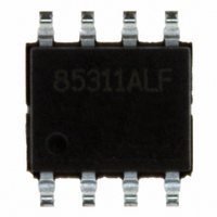
ICS85311AMLF IDT, Integrated Device Technology Inc, ICS85311AMLF Datasheet

ICS85311AMLF
Specifications of ICS85311AMLF
800-1166-5
800-1166
85311AMLF
Available stocks
Related parts for ICS85311AMLF
ICS85311AMLF Summary of contents
Page 1
LOW SKEW, 1-TO-2, DIFFERENTIAL-TO-LVPECL/ECL FANOUT BUFFER General Description The ICS85311 is a low skew, high perfor- mance ICS 1-to-2 Differential-to-2.5V/3.3V ECL/LVPECL Fanout Buffer and a member of the HiPerClockS™ HiPerClockS™ family of High Performance Clock Solutions from IDT. The CLK, ...
Page 2
ICS85311 LOW SKEW, 1-TO-2, DIFFERENTIAL-TO-LVPECL/ECLFANOUT BUFFER Table 1. Pin Descriptions Number Name 1, 2 Q0, nQ0 Output 3, 4 Q1, nQ1 Output 5 V Power EE 6 nCLK Input 7 CLK Input 8 V Power CC NOTE: Pullup and Pulldown ...
Page 3
ICS85311 LOW SKEW, 1-TO-2, DIFFERENTIAL-TO-LVPECL/ECLFANOUT BUFFER Absolute Maximum Ratings NOTE: Stresses beyond those listed under Absolute Maximum Ratings may cause permanent damage to the device. These ratings are stress specifications only. Functional operation of product at these conditions or any ...
Page 4
ICS85311 LOW SKEW, 1-TO-2, DIFFERENTIAL-TO-LVPECL/ECLFANOUT BUFFER Table 3C. LVPECL DC Characteristics, V Symbol Parameter V Output High Current; NOTE Output Low Current; NOTE Peak-to-Peak Output Voltage Swing SWING NOTE1: Outputs terminated with 50Ω to ...
Page 5
ICS85311 LOW SKEW, 1-TO-2, DIFFERENTIAL-TO-LVPECL/ECLFANOUT BUFFER Additive Phase Jitter (3.3V) The spectral purity in a band at a specific offset from the fundamental compared to the power of the fundamental is called the dBc Phase Noise. This value is normally ...
Page 6
ICS85311 LOW SKEW, 1-TO-2, DIFFERENTIAL-TO-LVPECL/ECLFANOUT BUFFER Parameter Measurement Information LVPECL V EE -1.3V ± 0.165V 3.3V Core/ 3.3V LVPECL Output Load AC Test Circuit V CC nCLK V Cross Points PP CLK V EE Differential Input Level ...
Page 7
ICS85311 LOW SKEW, 1-TO-2, DIFFERENTIAL-TO-LVPECL/ECLFANOUT BUFFER Parameter Measurement Information, continued nQ[0:1] Q[0: PERIOD t PW odc = t PERIOD Output Duty Cycle/Pulse Width/Period Application Information Wiring the Differential Input to Accept Single Ended Levels Figure 1 shows ...
Page 8
ICS85311 LOW SKEW, 1-TO-2, DIFFERENTIAL-TO-LVPECL/ECLFANOUT BUFFER Differential Clock Input Interface The CLK /nCLK accepts LVDS, LVPECL, LVHSTL, SSTL, HCSL and other differential signals. Both signals must meet the V V input requirements. Figures show interface CMR examples ...
Page 9
ICS85311 LOW SKEW, 1-TO-2, DIFFERENTIAL-TO-LVPECL/ECLFANOUT BUFFER Recommendations for Unused Output Pins Outputs: LVPECL Outputs All unused LVPECL outputs can be left floating. We recommend that there is no trace attached. Both sides of the differential output pair should either be ...
Page 10
ICS85311 LOW SKEW, 1-TO-2, DIFFERENTIAL-TO-LVPECL/ECLFANOUT BUFFER Termination for 2.5V LVPECL Outputs Figure 4A and Figure 4B show examples of termination for 2.5V LVPECL driver. These terminations are equivalent to terminating 50Ω – 2V. For V = 2.5V, the ...
Page 11
ICS85311 LOW SKEW, 1-TO-2, DIFFERENTIAL-TO-LVPECL/ECLFANOUT BUFFER Power Considerations This section provides information on power dissipation and junction temperature for the ICS85311. Equations and example calculations are also provided. 1. Power Dissipation. The total power dissipation for the ICS85311 is the ...
Page 12
ICS85311 LOW SKEW, 1-TO-2, DIFFERENTIAL-TO-LVPECL/ECLFANOUT BUFFER 3. Calculations and Equations. The purpose of this section is to derive the power dissipated into the load. LVPECL output driver circuit and termination are shown in Figure Figure 5. ...
Page 13
ICS85311 LOW SKEW, 1-TO-2, DIFFERENTIAL-TO-LVPECL/ECLFANOUT BUFFER Reliability Information Table 6. θ vs. Air Flow Table for a 8 Lead SOIC JA Linear Feet per Minute Single-Layer PCB, JEDEC Standard Test Boards Multi-Layer PCB, JEDEC Standard Test Boards NOTE: Most modern ...
Page 14
ICS85311 LOW SKEW, 1-TO-2, DIFFERENTIAL-TO-LVPECL/ECLFANOUT BUFFER Ordering Information Table 8. Ordering Information Part/Order Number Marking 85311AM 85311AM 85311AMT 85311AM 85311AMLF 85311ALF 85311AMLFT 85311ALF NOTE: Parts that are ordered with an "LF" suffix to the part number are the Pb-Free configuration ...
Page 15
ICS85311 LOW SKEW, 1-TO-2, DIFFERENTIAL-TO-LVPECL/ECLFANOUT BUFFER Revision History Sheet Rev Table Page Description of Change A 8 Added Termination for LVPECL Outputs section. 5 3.3V Output Load Test Circuit Diagram - corrected VEE equation to read A -1.3V ± 0.165V ...
Page 16
ICS85311 LOW SKEW, 1-TO-2, DIFFERENTIAL-TO-LVPECL/ECLFANOUT BUFFER Contact Information: www.IDT.com Sales 800-345-7015 (inside USA) +408-284-8200 (outside USA) Fax: 408-284-2775 www.IDT.com/go/contactIDT © 2008 Integrated Device Technology, Inc. All rights reserved. Product specifications subject to change without notice. IDT and the IDT logo ...


