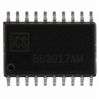
ICS853017AM IDT, Integrated Device Technology Inc, ICS853017AM Datasheet - Page 9

ICS853017AM
Manufacturer Part Number
ICS853017AM
Description
IC RCVR QUAD LVPECL/ECL 20-SOIC
Manufacturer
IDT, Integrated Device Technology Inc
Series
HiPerClockS™r
Type
Buffer/Driverr
Datasheet
1.ICS853017AM.pdf
(15 pages)
Specifications of ICS853017AM
Number Of Circuits
4
Ratio - Input:output
1:1
Differential - Input:output
Yes/Yes
Input
CML, LVDS, LVPECL, SSTL
Output
LVPECL
Frequency - Max
2GHz
Voltage - Supply
2.375 V ~ 5.25 V
Operating Temperature
-40°C ~ 85°C
Mounting Type
Surface Mount
Package / Case
20-SOIC (7.5mm Width)
Frequency-max
2GHz
Lead Free Status / RoHS Status
Contains lead / RoHS non-compliant
Other names
800-1161
800-1161-5
800-1161
853017AM
800-1161-5
800-1161
853017AM
T
The clock layout topology shown below is a typical termination
for LVPECL outputs. The two different layouts mentioned are
recommended only as guidelines.
FOUT and nFOUT are low impedance follower outputs that gen-
erate ECL/LVPECL compatible outputs. Therefore, terminating
resistors (DC current path to ground) or current sources must be
used for functionality. These outputs are designed to drive 50
T
This section shows examples of 5V LVPECL output termination.
Figure 4A shows standard termination for 5V LVPECL. The
termination requires matched load of 50
IDT
ERMINATION FOR
ERMINATION FOR
ICS853017
QUAD, 1-TO-1, DIFFERENTIAL-TO-2.5V, 3.3V, 5V LVPECL/ECL RECEIVER
F
RTT =
™
IGURE
/ ICS
5V
™
((V
4A. S
F
2.5V, 3.3V, 5V LVPECL/ECL RECEIVER
FOUT
OH
IGURE
PECL
+ V
TANDARD
OL
3A. LVPECL O
) / (V
Zo = 50 Ohm
Zo = 50 Ohm
1
3.3V LVPECL O
5V LVPECL O
CC
Z
Z
– 2)) – 2
o
o
5V LVPECL O
= 50
= 50
R1
50
Z
o
50
UTPUT
3V
UTPUT
T
UTPUTS
R2
50
UTPUT
ERMINATION
RTT
resistors pull down to
50
V
+
-
T
CC
ERMINATION
5V
FIN
- 2V
PECL
9
transmission lines. Matched impedance techniques should be
used to maximize operating frequency and minimize signal dis-
tortion. Figures 3A and 3B show two different layouts which are
recommended only as guidelines. Other suitable clock layouts
may exist and it would be recommended that the board design-
ers simulate to guarantee compatibility across all printed circuit
and clock component process variations.
V
equivalence of Figure 4A. In actual application where the 3V DC
power supply is not available, this approached is normally used.
CC
F
- 2V = 3V at the receiver. Figure 4B shows Thevenin
IGURE
FOUT
5V
F
4B. 5V LVPECL O
IGURE
PECL
3B. LVPECL O
Zo = 50 Ohm
Zo = 50 Ohm
Z
Z
o
o
= 50
= 50
ICS853017AM REV. B JANUARY 28, 2008
125
84
UTPUT
UTPUT
5V
R3
84
R1
125
3.3V
T
ERMINATION
R4
84
T
125
84
R2
125
ERMINATION
PRELIMINARY
FIN
+
-
E
XAMPLE
PECL


