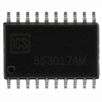
ICS853017AM IDT, Integrated Device Technology Inc, ICS853017AM Datasheet - Page 11

ICS853017AM
Manufacturer Part Number
ICS853017AM
Description
IC RCVR QUAD LVPECL/ECL 20-SOIC
Manufacturer
IDT, Integrated Device Technology Inc
Series
HiPerClockS™r
Type
Buffer/Driverr
Datasheet
1.ICS853017AM.pdf
(15 pages)
Specifications of ICS853017AM
Number Of Circuits
4
Ratio - Input:output
1:1
Differential - Input:output
Yes/Yes
Input
CML, LVDS, LVPECL, SSTL
Output
LVPECL
Frequency - Max
2GHz
Voltage - Supply
2.375 V ~ 5.25 V
Operating Temperature
-40°C ~ 85°C
Mounting Type
Surface Mount
Package / Case
20-SOIC (7.5mm Width)
Frequency-max
2GHz
Lead Free Status / RoHS Status
Contains lead / RoHS non-compliant
Other names
800-1161
800-1161-5
800-1161
853017AM
800-1161-5
800-1161
853017AM
This section provides information on power dissipation and junction temperature for the ICS853017.
Equations and example calculations are also provided.
1. Power Dissipation.
The total power dissipation for the ICS853017 is the sum of the core power plus the power dissipated in the load(s).
The following is the power dissipation for V
NOTE: Please refer to Section 3 for details on calculating power dissipated in the load.
2. Junction Temperature.
Junction temperature, Tj, is the temperature at the junction of the bond wire and bond pad and directly affects the reliability of the
device. The maximum recommended junction temperature for HiPerClockS
In order to calculate junction temperature, the appropriate junction-to-ambient thermal resistance
flow and a multi-layer board, the appropriate value is 46.2°C/W per Table 6 below.
Therefore, Tj for an ambient temperature of 85°C with all outputs switching is:
This calculation is only an example. Tj will obviously vary depending on the number of loaded outputs, supply voltage, air flow,
and the type of board (single layer or multi-layer).
T
IDT
ABLE
ICS853017
QUAD, 1-TO-1, DIFFERENTIAL-TO-2.5V, 3.3V, 5V LVPECL/ECL RECEIVER
™
The equation for Tj is as follows: Tj =
Tj = Junction Temperature
Pd_total = Total Device Power Dissipation (example calculation is in section 1 above)
T
85°C + 0.377W * 46.2°C/W = 102.4°C. This is well below the limit of 125°C.
/ ICS
JA
A
6. T
= Ambient Temperature
= Junction-to-Ambient Thermal Resistance
Single-Layer PCB, JEDEC Standard Test Boards
Multi-Layer PCB, JEDEC Standard Test Boards
NOTE: Most modern PCB designs use multi-layered boards. The data in the second row pertains to most designs.
Power (core)
Power (outputs)
If all outputs are loaded, the total power is 4 * 30.94mW = 123.76mW
Total Power
™
2.5V, 3.3V, 5V LVPECL/ECL RECEIVER
HERMAL
R
MAX
ESISTANCE
_MAX
= V
MAX
(5.5V, with all outputs switching) = 123.76mW + 253mW = 376.76mW
= 30.94mW/Loaded Output pair
CC_MAX
* I
JA
EE_MAX
FOR
= 5.5V * 46mA = 253mW
20-P
CC
JA
JA
= 5.5V, which gives worst case results.
P
IN
by Velocity (Linear Feet per Minute)
* Pd_total + T
SOIC, F
OWER
ORCED
C
A
ONSIDERATIONS
C
11
ONVECTION
83.2°C/W
46.2°C/W
0
TM
devices is 125°C.
65.7°C/W
39.7°C/W
200
ICS853017AM REV. B JANUARY 28, 2008
JA
must be used. Assuming no air
57.5°C/W
36.8°C/W
500
PRELIMINARY


