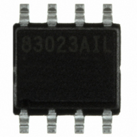
ICS83023AMILF IDT, Integrated Device Technology Inc, ICS83023AMILF Datasheet - Page 7

ICS83023AMILF
Manufacturer Part Number
ICS83023AMILF
Description
XLATOR/BUFFER DUAL 1:1 8-SOIC
Manufacturer
IDT, Integrated Device Technology Inc
Series
HiPerClockS™r
Type
Fanout Buffer (Distribution), Translatorr
Datasheet
1.ICS83023AMILF.pdf
(13 pages)
Specifications of ICS83023AMILF
Number Of Circuits
2
Ratio - Input:output
1:1
Differential - Input:output
Yes/No
Input
HCSL, LVDS, LVHSTL, LVPECL, SSTL
Output
LVCMOS, LVTTL
Frequency - Max
350MHz
Voltage - Supply
3 V ~ 3.6 V
Operating Temperature
-40°C ~ 85°C
Mounting Type
Surface Mount
Package / Case
8-SOIC
Frequency-max
350MHz
Number Of Outputs
2
Operating Supply Voltage (max)
3.6V
Operating Temp Range
-40C to 85C
Propagation Delay Time
2.4ns
Operating Supply Voltage (min)
3V
Mounting
Surface Mount
Pin Count
8
Operating Supply Voltage (typ)
3.3V
Package Type
SOIC N
Duty Cycle
57%
Operating Temperature Classification
Industrial
Lead Free Status / RoHS Status
Lead free / RoHS Compliant
Other names
800-1102
800-1102-5
800-1102
83023AMILF
800-1102-5
800-1102
83023AMILF
Available stocks
Company
Part Number
Manufacturer
Quantity
Price
Company:
Part Number:
ICS83023AMILF
Manufacturer:
IDT
Quantity:
2 000
Part Number:
ICS83023AMILFT
Manufacturer:
IDT
Quantity:
20 000
R
I
CLK/nCLK I
For applications not requiring the use of the differential input,
both CLK and nCLK can be left floating. Though not required,
but for additional protection, a 1k
CLK to ground.
83023AMI
W
Figure 1 shows how the differential input can be wired to accept
single ended levels. The reference voltage V_REF = V
generated by the bias resistors R1, R2 and C1. This bias circuit
should be located as close as possible to the input pin. The
NPUTS
ECOMMENDATIONS FOR
IRING THE
:
NPUT
D
IFFERENTIAL
:
U
NUSED
I
NPUT TO
F
IGURE
Single Ended Clock Input
resistor can be tied from
I
1. S
NPUT AND
A
A
CCEPT
PPLICATION
INGLE
E
O
C1
0.1u
NDED
S
UTPUT
INGLE
V_REF
DD
www.idt.com
S
D
/2 is
IGNAL
IFFERENTIAL
E
P
NDED
7
INS
I
D
ratio of R1 and R2 might need to be adjusted to position the
V_REF in the center of the input voltage swing. For example, if
the input clock swing is only 2.5V and V
be 1.25V and R2/R1 = 0.609.
NFORMATION
O
LVCMOS O
All unused LVCMOS output can be left floating. We
recommend that there is no trace attached.
RIVING
1K
R1
1K
R2
UTPUTS
VDD
L
EVELS
D
IFFERENTIAL
CLK
nCLK
-
:
TO
UTPUT
-LVCMOS T
:
I
NPUT
RANSLATOR
DD
ICS83023I
= 3.3V, V_REF should
D
UAL
REV. B JULY 29, 2010
/B
, 1-
UFFER
TO
-1


