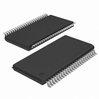
ICS9DB803DGLF IDT, Integrated Device Technology Inc, ICS9DB803DGLF Datasheet - Page 16

ICS9DB803DGLF
Manufacturer Part Number
ICS9DB803DGLF
Description
IC BUFFER 8OUTPUT DIFF 48-TSSOP
Manufacturer
IDT, Integrated Device Technology Inc
Type
Clock Bufferr
Series
-r
Datasheet
1.ICS9DB803DFLFT.pdf
(21 pages)
Specifications of ICS9DB803DGLF
Input
HCSL
Output
HCSL, LVDS
Frequency - Max
400MHz
Voltage - Supply
3.135 V ~ 3.465 V
Operating Temperature
0°C ~ 70°C
Mounting Type
Surface Mount
Package / Case
48-TSSOP
Frequency-max
400MHz
Number Of Elements
1
Supply Current
200mA
Pll Input Freq (min)
50MHz
Pll Input Freq (max)
110MHz
Operating Supply Voltage (typ)
3.3V
Operating Temp Range
0C to 70C
Package Type
TSSOP
Operating Supply Voltage (min)
3.135V
Operating Supply Voltage (max)
3.465V
Operating Temperature Classification
Commercial
Pin Count
48
Lead Free Status / RoHS Status
Lead free / RoHS Compliant
Other names
9DB803DGLF
Available stocks
Company
Part Number
Manufacturer
Quantity
Price
Part Number:
ICS9DB803DGLF
Manufacturer:
TI/德州仪器
Quantity:
20 000
Part Number:
ICS9DB803DGLFT
Manufacturer:
ICS
Quantity:
20 000
Note: Polarities in timing diagrams are shown OE_INV = 0. They are similar to OE_INV = 1.
PD#, Power Down
The PD# pin cleanly shuts off all clocks and places the device into a power saving mode. PD# must be asserted before shutting
off the input clock or power to insure an orderly shutdown. PD is asynchronous active-low input for both powering down the
device and powering up the device. When PD# is asserted, all clocks will be driven high, or tri-stated (depending on the PD#
drive mode and Output control bits) before the PLL is shut down.
PD# Assertion
When PD# is sampled low by two consecutive rising edges of DIF#, all DIF outputs must be held High, or tri-stated (depending
on the PD# drive mode and Output control bits) on the next High-Low transition of the DIF# outputs. When the PD# drive mode
bit is set to ‘0’, all clock outputs will be held with DIF driven High with 2 x I
set to ‘1’, both DIF and DIF# are tri-stated.
PD# De-assertion
Power-up latency is less than 1 ms. This is the time from de-assertion of the PD# pin, or VDD reaching 3.3V, or the time from
valid SRC_IN clocks until the time that stable clocks are output from the device (PLL Locked). If the PD# drive mode bit is set
to ‘1’, all the DIF outputs must driven to a voltage of >200 mV within 300 us of PD# de-assertion.
IDT
ICS9DB803D
Eight Output Differential Buffer for PCIe for Gen 2
TM
/ICS
TM
Eight Output Differential Buffer for PCIe Gen 2
PWRDWN#
PWRDWN#
DIF#
DIF#
DIF
DIF
Tstable
<1mS
<300uS, >200mV
Tdrive_PwrDwn#
16
REF
and DIF# tri-stated. If the PD# drive mode bit is
ICS9DB803D
REV J 01/27/11


