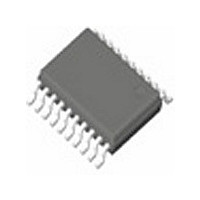
ICS9DB102BGLF IDT, Integrated Device Technology Inc, ICS9DB102BGLF Datasheet - Page 2

ICS9DB102BGLF
Manufacturer Part Number
ICS9DB102BGLF
Description
IC BUFFER PCI EXPRESS 20-TSSOP
Manufacturer
IDT, Integrated Device Technology Inc
Type
Zero Delay Bufferr
Series
-r
Datasheet
1.ICS9DB102BFLFT.pdf
(13 pages)
Specifications of ICS9DB102BGLF
Input
Clock
Output
HCSL
Frequency - Max
101MHz
Voltage - Supply
3.135 V ~ 3.465 V
Operating Temperature
0°C ~ 70°C
Mounting Type
Surface Mount
Package / Case
20-TSSOP
Frequency-max
101MHz
Number Of Elements
1
Supply Current
100mA
Pll Input Freq (min)
80MHz
Pll Input Freq (max)
105MHz
Operating Supply Voltage (typ)
3.3V
Operating Temp Range
0C to 70C
Package Type
TSSOP
Operating Supply Voltage (min)
3.135V
Operating Supply Voltage (max)
3.465V
Operating Temperature Classification
Commercial
Pin Count
20
Lead Free Status / RoHS Status
Lead free / RoHS Compliant
Lead Free Status / RoHS Status
Compliant, Lead free / RoHS Compliant
Other names
9DB102BGLF
Available stocks
Company
Part Number
Manufacturer
Quantity
Price
Company:
Part Number:
ICS9DB102BGLF
Manufacturer:
ICS
Quantity:
5 072
Part Number:
ICS9DB102BGLFT
Manufacturer:
IDT
Quantity:
20 000
Pin Configuration
Pin Description
IDT
Note:
Pins preceeded by '**' have internal 120K ohm pull down resistors
PIN #
ICS9DB102
Two Output Differential Buffer for PCIe Gen1 & Gen2
®
**CLKREQ0# 4
10
11
12
13
14
15
16
17
18
19
20
1
2
3
4
5
6
7
8
9
Two Output Differential Buffer for PCIe Gen1 & Gen2
PCIEXC0 8
CLK_INC 3
PCIEXT0 7
SMBDAT 10
CLK_INT 2
Note: Pins preceeded by '**' have internal
PLL_BW 1
PLL_BW
CLK_INT
CLK_INC
**CLKREQ0#
VDD
GND
PCIEXT0
PCIEXC0
VDD
SMBDAT
SMBCLK
VDD
PCIEXC1
PCIEXT1
GND
VDD
**CLKREQ1#
IREF
GNDA
VDDA
GND 6
VDD 5
VDD 9
20-pin SSOP & TSSOP
120K ohm pull down resistors
PIN NAME
PIN TYPE
OUTPUT
OUTPUT
OUTPUT
OUTPUT
OUTPUT
POWER
POWER
POWER
POWER
POWER
POWER
POWER
POWER
INPUT
INPUT
INPUT
INPUT
INPUT
INPUT
20 VDDA
19 GNDA
18 IREF
17 **CLKREQ1#
16 VDD
15 GND
14 PCIEXT1
13 PCIEXC1
12 VDD
11 SMBCLK
I/O
3.3V input for selecting PLL Band Width
0 = low, 1= high
"True" reference clock input.
"Complementary" reference clock input.
Output enable for SRC/PCI Express output pair '0'
0 = enabled, 1 = tri-stated
Power supply, nominal 3.3V
Ground pin.
True clock of differential PCI_Express pair.
Complement clock of differential PCI_Express pair.
Power supply, nominal 3.3V
Data pin of SMBUS circuitry, 5V tolerant
Clock pin of SMBUS circuitry, 5V tolerant
Power supply, nominal 3.3V
Complement clock of differential PCI_Express pair.
True clock of differential PCI_Express pair.
Ground pin.
Power supply, nominal 3.3V
Output enable for SRC/PCI Express output pair '1'
0 = enabled, 1 = tri-stated
This pin establishes the reference current for the differential current-
mode output pairs. This pin requires a fixed precision resistor tied to
ground in order to establish the appropriate current. 475 ohms is the
standard value.
Ground pin for the PLL core.
3.3V power for the PLL core.
2
Power Groups
5,9,12,16
VDD
20
20
9
Pin Number
DESCRIPTION
GND
6,15
19
19
6
Analog VDD & GND for PLL core
PCI Express Outputs
Description
852
SMBUS
IREF
REV M 01/27/11


