ICS9FG104DGILFT IDT, Integrated Device Technology Inc, ICS9FG104DGILFT Datasheet - Page 4
ICS9FG104DGILFT
Manufacturer Part Number
ICS9FG104DGILFT
Description
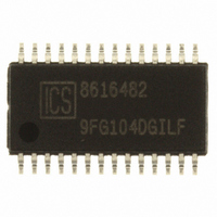
IC FREQ TIMING GENERATOR 28TSSOP
Manufacturer
IDT, Integrated Device Technology Inc
Type
Frequency Generatorr
Datasheet
1.ICS9FG104DFLFT.pdf
(17 pages)
Specifications of ICS9FG104DGILFT
Input
Clock, Crystal
Output
Differential
Frequency - Max
400MHz
Voltage - Supply
3.135 V ~ 3.465 V
Operating Temperature
-40°C ~ 85°C
Mounting Type
Surface Mount
Package / Case
28-TSSOP
Frequency-max
400MHz
Lead Free Status / RoHS Status
Lead free / RoHS Compliant
Other names
800-1255-2
9FG104DGILFT
9FG104DGILFT


Absolute Max
IDT
Tambient Ambient Operating Temp•(Commerical Grade)
Tambient
T
Operating Supply Current
Input Rise and Fall times
1
2
3
4
will scale these frequencies accordingly. The output frequecy selected by the FS inputs will also scale.
For example, 27MHz input with an FS selection of 100MHz will yield an output frequency of 27/25 x 100 =
108MHz.
ESD prot
Electrical Characteristics - Input/Supply/Common Output Parameters
Symbol
ppm frequency accuracy on PLL outputs.
Guaranteed by design, not 100% tested in production.
See timing diagrams for timing requirements.
VDDxx
Tcase
A
Input frequency should be measured at the REF pin and tuned to 0 PPM to meet
These values assume 25MHz or 14.31818MHz inputs respectively. Using a higher or lower frequency
ICS9FG104D
Frequency Generator for CPU, QPI, FBD, PCIe Gen 2 & SATA
Modulation Frequency
Modulation Frequency
®
= T
Input High Voltage
Clk Stabilization
Input High Current
Ts
Input Low Voltage
DIF output enable
Frequency Generator for CPU, QPI, FBD, PCIe Gen 2 & SATA
Input Low Current
Input Frequency
Pin Inductance
PARAMETER
Capacitance
Input/Output
A M B IENT
Ambient Operating Temp•(Industrial Grade)
Input ESD protection•human body model
; Supply Voltage V
1
1,2
1
3
Storage Temperature
3.3V Supply Voltage
Case Temperature
SYMBOL
I
T
DD3.3STOP
I
T
Parameter
DD3.3OP
STABcom
t
C
STABind
f
f
DIFOE
t
V
L
C
V
I
I
MOD
MOD
R
I
F
IL1
IL2
OUT
IH
pin
/t
IH
IN
IL
i
DD
F
= 3.3 V +/-5%
V
V
IN
Full Active, C
Full Active, C
All outputs stopped driven
From V
From V
IN
All outputs stopped Hi-Z
DIF_Stop# de-assertion
Output pin capacitance
DIF output enable after
= 0 V; Inputs with no pull-
= 0 V; Inputs with pull-up
20% to 80% of VDD
SEL14M_25M# = 0
SEL14M_25M# = 1
clock (Commercial)
SEL14M_25M# = 0
SEL14M_25M# = 1
clock (Industrial)
CONDITIONS
f = 400 MHz
f = 100 MHz
Logic Inputs
3.3 V +/-5%
3.3 V +/-5%
up resistors
DD
DD
V
resistors
IN
Power-Up to 1st
Power-Up to 1st
= V
L
L
= Full load;
= Full load;
DD
2000
4
Min
-65
-40
0
V
12.886 14.31818
SS
-200
22.5
MIN
1.5
-5
-5
2
- 0.3
Max
+70
+85
150
115
4.6
32.541
32.467
25.00
TYP
125
110
106
48
V
15.75
Units
MAX
DD
27.5
150
125
120
0.8
1.8
1.8
60
15
°
°C
°C
°C
V
V
5
7
5
6
5
+ 0.3
C
UNITS NOTES
MHz
MHz
kHz
kHz
mA
mA
mA
mA
ms
ms
uA
uA
uA
nH
pF
pF
ns
ns
V
V
1,3,4
1,3,4
1,2
1,2
1
1
1
1
1
1
1
1
1
3
3
1
1
1
1
1
1541C—12/16/10
Related parts for ICS9FG104DGILFT
Image
Part Number
Description
Manufacturer
Datasheet
Request
R

Part Number:
Description:
TRANSLATION DEVICE DPI 80-PQFP
Manufacturer:
IDT, Integrated Device Technology Inc
Datasheet:
Part Number:
Description:
IDT PART
Manufacturer:
IDT, Integrated Device Technology Inc
Datasheet:
Part Number:
Description:
IC LIU T1/E1/J1 OCTAL 256PBGA
Manufacturer:
IDT, Integrated Device Technology Inc
Datasheet:
Part Number:
Description:
IC CLK DVR PLL 1:10 40VFQFPN
Manufacturer:
IDT, Integrated Device Technology Inc
Datasheet:
Part Number:
Description:
IC CLK FANOUT BUFFER 1:18 32LQFP
Manufacturer:
IDT, Integrated Device Technology Inc
Datasheet:
Part Number:
Description:
IC CLK FANOUT BUFFER 1:18 32LQFP
Manufacturer:
IDT, Integrated Device Technology Inc
Datasheet:
Part Number:
Description:
IC CK505 VREG/RES 56TSSOP
Manufacturer:
IDT, Integrated Device Technology Inc
Datasheet:

Part Number:
Description:
IC SDRAM CLK DVR 1:10 48-TSSOP
Manufacturer:
IDT, Integrated Device Technology Inc
Datasheet:

Part Number:
Description:
IC CLK DVR PLL 1:10 48TSSOP
Manufacturer:
IDT, Integrated Device Technology Inc
Datasheet:
Part Number:
Description:
IC FLEXPC CLK PROGR P4 56-TSSOP
Manufacturer:
IDT, Integrated Device Technology Inc
Datasheet:
Part Number:
Description:
IC FLEXPC CLK PROGR P4 56-TSSOP
Manufacturer:
IDT, Integrated Device Technology Inc
Datasheet:
Part Number:
Description:
IC FLEXPC CLK PROGR P4 56-SSOP
Manufacturer:
IDT, Integrated Device Technology Inc
Datasheet:

Part Number:
Description:
IC PLL CLK DRIVER 2.5V 28-TSSOP
Manufacturer:
IDT, Integrated Device Technology Inc
Datasheet:
Part Number:
Description:
IC CLOCK DRIVER 2.5V 24-TSSOP
Manufacturer:
IDT, Integrated Device Technology Inc
Datasheet:
Part Number:
Description:
IC TIMING CTRL HUB K7 48-SSOP
Manufacturer:
IDT, Integrated Device Technology Inc
Datasheet: