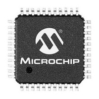
PIC24FV32KA304-I/PT Microchip Technology, PIC24FV32KA304-I/PT Datasheet - Page 223

PIC24FV32KA304-I/PT
Manufacturer Part Number
PIC24FV32KA304-I/PT
Description
MCU 32KB FLASH 2KB RAM 44-TQFP
Manufacturer
Microchip Technology
Specifications of PIC24FV32KA304-I/PT
Processor Series
PIC24FV
Core
PIC
Data Bus Width
16 bit
Program Memory Type
Flash
Program Memory Size
32 KB
Data Ram Size
2 KB
Maximum Operating Temperature
+ 85 C
Mounting Style
SMD/SMT
Package / Case
TQFP-44
Development Tools By Supplier
MPLAB IDE Software
Minimum Operating Temperature
- 40 C
Lead Free Status / Rohs Status
Lead free / RoHS Compliant
Available stocks
Company
Part Number
Manufacturer
Quantity
Price
Company:
Part Number:
PIC24FV32KA304-I/PT
Manufacturer:
VISHAY
Quantity:
12 000
Company:
Part Number:
PIC24FV32KA304-I/PT
Manufacturer:
Microchip Technology
Quantity:
10 000
- Current page: 223 of 320
- Download datasheet (3Mb)
22.2
The analog input model of the 12-bit A/D Converter is
shown in
A/D is a function of the holding capacitor charge time.
For the A/D Converter to meet its specified accuracy,
the charge holding capacitor (C
to fully charge to the voltage level on the analog input
pin. The source impedance (R
impedance (R
(R
required to charge C
the analog sources must, therefore, be small enough to
fully charge the holding capacitor within the chosen
sample time. To minimize the effects of pin leakage
currents on the accuracy of the A/D Converter, the
maximum recommended source impedance, R
2.5 k. After the analog input channel is selected
(changed), this sampling function must be completed
FIGURE 22-2:
2011 Microchip Technology Inc.
SS
) impedance combine to directly affect the time
A/D Sampling Requirements
Figure
Note: C
IC
) and the internal sampling switch
22-2. The total sampling time for the
PIN
VA
HOLD
value depends on device package and is not tested. Effect of C
Rs
12-BIT A/D CONVERTER ANALOG INPUT MODEL
. The combined impedance of
ANx
C
PIN
Legend: C
HOLD
S
), the interconnect
) must be allowed
V
I
R
R
C
LEAKAGE
T
PIN
IC
SS
HOLD
= Input Capacitance
= Threshold Voltage
= Leakage Current at the pin due to
= Interconnect Resistance
= Sampling Switch Resistance
= Sample-and-Hold Capacitance (from DAC)
S
PIC24FV32KA304 FAMILY
various junctions
, is
R
I
500 nA
prior to starting the conversion. The internal holding
capacitor will be in a discharged state prior to each
sample operation.
At least 1 T
conversions for the sample time. For more details, see
Section 29.0 “Electrical
EQUATION 22-1:
LEAKAGE
IC
Note:
250
AD
Based on T
and PLL are disabled.
PIN
Sampling
time period should be allowed between
T
Switch
ADCS
AD
negligible if Rs 5 k.
R
=
SS
T
A/D CONVERSION CLOCK
PERIOD
=
CY
CY
T
--------- - 1
T
R
Characteristics”.
AD
CY
SS
ADCS
= 2/F
V
3 k
–
SS
C
= 4.4 pF
HOLD
OSC
+
DS39995B-page 223
1
; Doze mode
Related parts for PIC24FV32KA304-I/PT
Image
Part Number
Description
Manufacturer
Datasheet
Request
R

Part Number:
Description:
Manufacturer:
Microchip Technology Inc.
Datasheet:

Part Number:
Description:
Manufacturer:
Microchip Technology Inc.
Datasheet:

Part Number:
Description:
Manufacturer:
Microchip Technology Inc.
Datasheet:

Part Number:
Description:
Manufacturer:
Microchip Technology Inc.
Datasheet:

Part Number:
Description:
Manufacturer:
Microchip Technology Inc.
Datasheet:

Part Number:
Description:
Manufacturer:
Microchip Technology Inc.
Datasheet:

Part Number:
Description:
Manufacturer:
Microchip Technology Inc.
Datasheet:

Part Number:
Description:
Manufacturer:
Microchip Technology Inc.
Datasheet:


