PIC24FV32KA304-I/PT Microchip Technology, PIC24FV32KA304-I/PT Datasheet - Page 219
PIC24FV32KA304-I/PT
Manufacturer Part Number
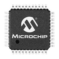
PIC24FV32KA304-I/PT
Description
MCU 32KB FLASH 2KB RAM 44-TQFP
Manufacturer
Microchip Technology
Specifications of PIC24FV32KA304-I/PT
Processor Series
PIC24FV
Core
PIC
Data Bus Width
16 bit
Program Memory Type
Flash
Program Memory Size
32 KB
Data Ram Size
2 KB
Maximum Operating Temperature
+ 85 C
Mounting Style
SMD/SMT
Package / Case
TQFP-44
Development Tools By Supplier
MPLAB IDE Software
Minimum Operating Temperature
- 40 C
Lead Free Status / Rohs Status
Lead free / RoHS Compliant
Available stocks
Company
Part Number
Manufacturer
Quantity
Price
Company:

Part Number:
PIC24FV32KA304-I/PT
Manufacturer:
VISHAY
Quantity:
12 000
Company:
Part Number:
PIC24FV32KA304-I/PT
Manufacturer:
Microchip Technology
Quantity:
10 000


REGISTER 22-5:
2011 Microchip Technology Inc.
bit 15
bit 7
Legend:
R = Readable bit
-n = Value at POR
bit 15-13
bit 12-8
bit 7-5
bit 4-0
Note 1:
CH0NB2
CH0NA2
R/W-0
R/W-0
2:
3:
Implemented on 44-pin devices only.
Implemented on 28-pin and 44-pin devices only.
Actual band gap value used for this input is selected by the PVCFG bits (AD1CON2<15:14>).
CH0NB<2:0>: Sample B Channel 0 Negative Input Select bits
111 = AN6
110 = AN5
101 = AN4
100 = AN3
011 = AN2
010 = AN1
001 = AN0
000 = AV
CH0SB<4:0>: S/H Amplifier Positive Input Select for MUX B Multiplexer Setting bits
11111 = Unimplemented, do not use
11101 = AV
11101 = AV
11100 = Upper guardband rail (0.785 * V
11011 = Lower guardband rail (0.215 * V
11010 = Internal Band Gap Reference (V
11001-10010 = Unimplemented, do not use
10001 = No channels connected, all inputs floating (used for CTMU)
10000 = No channels connected, all inputs floating (used for CTMU Temperature Sensor input)
01111 = AN15
01110 = AN14
01101 = AN13
01100 = AN12
01011 = AN11
01010 = AN10
01001 = AN9
01000 = AN8
00111 = AN7
00110 = AN6
00101 = AN5
00100 = AN4
00011 = AN3
00010 = AN2
00001 = AN1
00000 = AN0
CH0NA<2:0>: Sample A Channel 0 Negative Input Select bits
Same definitions as for CHONB<2:0>.
CH0SA<4:0>: Sample A Channel 0 Positive Input Select bits
Same definitions as for CHONA<4:0>.
CH0NB1
CH0NA1
R/W-0
R/W-0
AD1CHS: A/D SAMPLE SELECT REGISTER
SS
(1)
(2)
DD
SS
(1)
(1)
(1)
(2)
W = Writable bit
‘1’ = Bit is set
(3)
(3)
CH0NB0
CH0NA0
R/W-0
R/W-0
CH0SB4
CH0SA4
R/W-0
R/W-0
PIC24FV32KA304 FAMILY
DD
DD
BG
)
)
U = Unimplemented bit, read as ‘0’
‘0’ = Bit is cleared
)
(3)
CH0SB3
CH0SA3
R/W-0
R/W-0
CH0SB2
CH0SA2
R/W-0
R/W-0
x = Bit is unknown
CH0SB1
CH0SA1
R/W-0
R/W-0
DS39995B-page 219
CH0SB0
CH0SA0
R/W-0
R/W-0
bit 8
bit 0
Related parts for PIC24FV32KA304-I/PT
Image
Part Number
Description
Manufacturer
Datasheet
Request
R

Part Number:
Description:
Manufacturer:
Microchip Technology Inc.
Datasheet:
Part Number:
Description:
Manufacturer:
Microchip Technology Inc.
Datasheet:
Part Number:
Description:
Manufacturer:
Microchip Technology Inc.
Datasheet:
Part Number:
Description:
Manufacturer:
Microchip Technology Inc.
Datasheet:
Part Number:
Description:
Manufacturer:
Microchip Technology Inc.
Datasheet:
Part Number:
Description:
Manufacturer:
Microchip Technology Inc.
Datasheet:
Part Number:
Description:
Manufacturer:
Microchip Technology Inc.
Datasheet:
Part Number:
Description:
Manufacturer:
Microchip Technology Inc.
Datasheet: