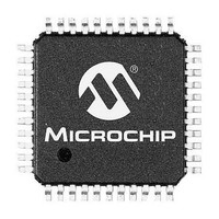
PIC24FV32KA304-I/PT Microchip Technology, PIC24FV32KA304-I/PT Datasheet - Page 218

PIC24FV32KA304-I/PT
Manufacturer Part Number
PIC24FV32KA304-I/PT
Description
MCU 32KB FLASH 2KB RAM 44-TQFP
Manufacturer
Microchip Technology
Specifications of PIC24FV32KA304-I/PT
Processor Series
PIC24FV
Core
PIC
Data Bus Width
16 bit
Program Memory Type
Flash
Program Memory Size
32 KB
Data Ram Size
2 KB
Maximum Operating Temperature
+ 85 C
Mounting Style
SMD/SMT
Package / Case
TQFP-44
Development Tools By Supplier
MPLAB IDE Software
Minimum Operating Temperature
- 40 C
Lead Free Status / Rohs Status
Lead free / RoHS Compliant
Available stocks
Company
Part Number
Manufacturer
Quantity
Price
Company:
Part Number:
PIC24FV32KA304-I/PT
Manufacturer:
VISHAY
Quantity:
12 000
Company:
Part Number:
PIC24FV32KA304-I/PT
Manufacturer:
Microchip Technology
Quantity:
10 000
- Current page: 218 of 320
- Download datasheet (3Mb)
PIC24FV32KA304 FAMILY
REGISTER 22-4:
DS39995B-page 218
bit 15
bit 7
Legend:
R = Readable bit
-n = Value at POR
bit 15
bit 14
bit 13
bit 12
bit 11
bit 10
bit 9-8
bit 7-4
bit 3-2
bit 1-0
R/W-0
ASEN
U-0
—
ASEN: Auto-Scan Enable bit
1 = Auto-scan is enabled
0 = Auto-scan is disabled
LPEN: Low-Power Enable bit
1 = Return to Low-Power mode after scan
0 = Remain in Full-Power mode after scan
CTMREQ: CTMU Request bit
1 = CTMU is enabled when the ADC is enabled and active
0 = CTMU is not enabled by the ADC
BGREQ: Band Gap Request bit
1 = Band gap is enabled when the ADC is enabled and active
0 = Band gap is not enabled by the ADC
VRSREQ: VREG Scan Request bit
1 = On-chip regulator is enabled when the ADC is enabled and active
0 = On-chip regulator is not enabled by the ADC
Unimplemented: Read as ‘0’
ASINT<1:0>: Auto-Scan (Threshold Detect) Interrupt Mode bits
11 = Interrupt after Threshold Detect sequence completed and valid compare has occurred
10 = Interrupt after valid compare has occurred
01 = Interrupt after Threshold Detect sequence completed
00 = No interrupt
Unimplemented: Read as ‘0’
WM<1:0>: Write Mode bits
11 = Reserved
10 = Auto-compare only (conversion results are not saved, but interrupts are generated when a valid
01 = Convert and save (conversion results are saved to locations as determined by register bits when
00 = Legacy operation (conversion data saved to location determined by buffer register bits)
CM<1:0>: Compare Mode bits
11 = Outside Window mode (valid match occurs if the conversion result is outside of the window defined by
10 = Inside Window mode (valid match occurs if the conversion result is inside the window defined by the
01 = Greater Than mode (valid match occurs if the result is greater than value in the corresponding buffer
00 = Less Than mode (valid match occurs if the result is less than value in the corresponding buffer register)
R/W-0
LPEN
U-0
—
match, as defined by CM and ASINT bits, occurs)
a match, as defined by CM bits, occurs)
the corresponding buffer pair)
corresponding buffer pair)
register)
AD1CON5: A/D CONTROL REGISTER 5
W = Writable bit
‘1’ = Bit is set
CTMREQ
R/W-0
U-0
—
BGREQ
R/W-0
U-0
—
U = Unimplemented bit, read as ‘0’
‘0’ = Bit is cleared
VRSREQ
R/W-0
R/W-0
WM1
R/W-0
WM0
U-0
—
2011 Microchip Technology Inc.
x = Bit is unknown
ASINT1
R/W-0
R/W-0
CM1
ASINT0
R/W-0
R/W-0
CM0
bit 8
bit 0
Related parts for PIC24FV32KA304-I/PT
Image
Part Number
Description
Manufacturer
Datasheet
Request
R

Part Number:
Description:
Manufacturer:
Microchip Technology Inc.
Datasheet:

Part Number:
Description:
Manufacturer:
Microchip Technology Inc.
Datasheet:

Part Number:
Description:
Manufacturer:
Microchip Technology Inc.
Datasheet:

Part Number:
Description:
Manufacturer:
Microchip Technology Inc.
Datasheet:

Part Number:
Description:
Manufacturer:
Microchip Technology Inc.
Datasheet:

Part Number:
Description:
Manufacturer:
Microchip Technology Inc.
Datasheet:

Part Number:
Description:
Manufacturer:
Microchip Technology Inc.
Datasheet:

Part Number:
Description:
Manufacturer:
Microchip Technology Inc.
Datasheet:


