HW-FMC-XM104-G Xilinx Inc, HW-FMC-XM104-G Datasheet - Page 15
HW-FMC-XM104-G
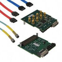
Manufacturer Part Number
HW-FMC-XM104-G
Description
CARD, CONNECTIVITY, FMC XM104
Manufacturer
Xilinx Inc
Datasheet
1.HW-FMC-XM104-G.pdf
(20 pages)
Specifications of HW-FMC-XM104-G
Kit Contents
FMC XM104 Connectivity Card, 4x SMA To SMA Cables, SATA Cable, Welcome Letter
Features
VITA 57.1 FMC High Pin Count (HPC) Connector
Accessory Type
Interface Board
Lead Free Status / RoHS Status
Lead free / RoHS Compliant
For Use With/related Products
Xilinx FMC-Supported Boards
Lead Free Status / RoHS Status
Lead free / RoHS Compliant, Lead free / RoHS Compliant
Other names
122-1693


Table 1-7: FPGA Multi-Gigabit Transceiver Data Ports 4 - 7 Connectivity
FMC XM104 Connectivity Card User Guide
UG536 (v1.1) September 24, 2010
Notes:
1. All receiver signals are AC coupled using 0.1 uF series capacitors
Connector J1 Pin
FMC HPC
A14
A15
A18
A19
B16
B17
B12
B13
6. Multi-Gigabit Transceiver Data Ports [4:7] - J2 10GE Base-CX4 Connector
7. 2 Kb EEPROM
DP4_M2C_N
DP5_M2C_N
DP6_M2C_N
DP7_M2C_N
DP4_M2C_P
DP5_M2C_P
DP6_M2C_P
DP7_M2C_P
Signal Name
Board FPGA multi-gigabit transceiver Data Ports 4 through 7 are wired to a 10GE Base-
CX4 connector J2 on the XM104. The four data port connections between the XM104 FMC
HPC connector and the 10G Base-CX4 connector J2 are defined in
An STMicroelectronics M24C02 2 Kb serial IIC bus EEPROM component provides a small
amount of non-volatile memory storage on the XM104. The IIC interface is connected
directly to the board’s IIC interface as shown in
The IIC address of this component is controlled by a combination of the board’s interface
and chip enable connections to the component inputs on the XM104. Signals GA0 and GA1
from the board are connected to the chip enable inputs of the M24C02 component enables
E0 and E1. Xilinx boards provide GA0 and GA1 signal strapping to 3.3V and GND signals
creating different E0 and E1 chip enable decodes on the E1 and E0 inputs of the EEPROM.
The IIC memory addressing protocol requires a bus master to initiate communication to a
peripheral device using a start condition followed by a device select code. The device select
code consists of a 4 bit Device Type Identifier and a 3-bit Chip Enable Address (E2, E1 and
E0). Bit 0 is used to indicate read/write. The Device Type Identifier for the EEPROM is 1010
binary.
Code Select addresses of the EEPROM when the XM104 is connected to a Xilinx board
defined in
Table 1-8: EEPROM IIC Device Select Code
The M24C02 component data sheet is available online at www.st.com.
Type Identifier
Bit 7:4 Device
1010
Table 1-8
(1)
(1)
(1)
(1)
(1)
(1)
(1)
(1)
Table 1-1, page
J2 Connector Pin
defines the generic EEPROM Device Select Code as well as specific Device
Bit 3
(Receiver)
0
S1
S2
S3
S4
S5
S6
S7
S8
Bit 2
GA0
www.xilinx.com
7.
Bit 1
GA1
Connector J1 Pin
FMC HPC
Read/Write
A39
A38
A35
A34
B33
B32
B37
B36
Bit 0 LSB
Figure 1-2, page
Signal Name
Connected to mezzanine FMC HPC
interface
DP7_C2M_N
DP6_C2M_N
DP5_C2M_N
DP4_C2M_N
DP7_C2M_P
DP6_C2M_P
DP5_C2M_P
DP4_C2M_P
Board Technical Description
10.
Description
Table
J2 Connector Pin
1-7.
(Transmitter)
S10
S11
S12
S13
S14
S15
S16
S9
15
Related parts for HW-FMC-XM104-G
Image
Part Number
Description
Manufacturer
Datasheet
Request
R

Part Number:
Description:
CARD, CONNECTIVITY, FMC XM105
Manufacturer:
Xilinx Inc
Datasheet:
Part Number:
Description:
HARDWARE FMC-VIDEO DAUGHTER CARD
Manufacturer:
Xilinx Inc
Datasheet:
Part Number:
Description:
HARDWARE FMC INTERFACE CARD
Manufacturer:
Xilinx Inc
Datasheet:

Part Number:
Description:
IC CPLD .8K 36MCELL 44-VQFP
Manufacturer:
Xilinx Inc
Datasheet:

Part Number:
Description:
IC CPLD 72MCRCELL 10NS 44VQFP
Manufacturer:
Xilinx Inc
Datasheet:

Part Number:
Description:
IC CPLD 1.6K 72MCELL 64-VQFP
Manufacturer:
Xilinx Inc
Datasheet:

Part Number:
Description:
IC CR-II CPLD 64MCELL 44-VQFP
Manufacturer:
Xilinx Inc
Datasheet:

Part Number:
Description:
IC CPLD 1.6K 72MCELL 100-TQFP
Manufacturer:
Xilinx Inc
Datasheet:

Part Number:
Description:
IC CR-II CPLD 64MCELL 56-BGA
Manufacturer:
Xilinx Inc
Datasheet:

Part Number:
Description:
IC CPLD 72MCRCELL 7.5NS 44VQFP
Manufacturer:
Xilinx Inc
Datasheet:
Part Number:
Description:
IC CR-II CPLD 64MCELL 100-VQFP
Manufacturer:
Xilinx Inc
Datasheet:
Part Number:
Description:
IC CPLD 1.6K 72MCELL 100-TQFP
Manufacturer:
Xilinx Inc
Datasheet:

Part Number:
Description:
IC CPLD 72MCRCELL 7.5NS 64VQFP
Manufacturer:
Xilinx Inc
Datasheet:
Part Number:
Description:
IC CPLD 1.6K 72MCELL 100-TQFP
Manufacturer:
Xilinx Inc
Datasheet:

Part Number:
Description:
IC CPLD 1.5K 64MCELL HP 44-VQFP
Manufacturer:
Xilinx Inc