HW-FMC-XM104-G Xilinx Inc, HW-FMC-XM104-G Datasheet - Page 10
HW-FMC-XM104-G
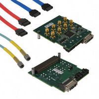
Manufacturer Part Number
HW-FMC-XM104-G
Description
CARD, CONNECTIVITY, FMC XM104
Manufacturer
Xilinx Inc
Datasheet
1.HW-FMC-XM104-G.pdf
(20 pages)
Specifications of HW-FMC-XM104-G
Kit Contents
FMC XM104 Connectivity Card, 4x SMA To SMA Cables, SATA Cable, Welcome Letter
Features
VITA 57.1 FMC High Pin Count (HPC) Connector
Accessory Type
Interface Board
Lead Free Status / RoHS Status
Lead free / RoHS Compliant
For Use With/related Products
Xilinx FMC-Supported Boards
Lead Free Status / RoHS Status
Lead free / RoHS Compliant, Lead free / RoHS Compliant
Other names
122-1693


Chapter 1: XM104
Board Technical Description
10
The XM104 provides a number of connectors which break out the FPGA multi-gigabit
transceiver (MGT) interface signals to and from the board interface.
block diagram of the XM104. Each MGT data port interface consists of two differential
pairs of MGT signals, one pair for the transmitter and one pair for the receiver. MGT Data
Ports 0 and 1 are each wired to four SMA connectors. MGT Data Ports 2 and 3 are each
wired to host Serial ATA connectors J11 and J12 respectively. MGT Data Ports 4 through 7
are wired to a 10GE Base-CX4 connector supporting a XAUI application interface. MGT
transmitter Data Ports 8 and 9 are electrically looped back to the board receiver ports 8 and
9 respectively. The ML605 does not support Data Port 8 and 9 interfaces.
Silicon Laboratories Si570 serial IIC bus reprogrammable LVDS clock source and a Si5368
any-rate precision clock multiplier and jitter attenuator integrated circuits provide a
variety of programmable differential clock sources to the board’s FGPA. The Si5368
integrated circuit receives three differential LVDS clock inputs from the board and outputs
five LVDS differential clock outputs to the FPGA.
A 2 Kb serial IIC EEPROM is also connected to the IIC interface of the board providing
non-volatile storage. The serial IIC interface also connects to the Si570 and Si5368
integrated circuits enabling the board’s FPGA to program the clock circuitry on the XM104.
X-Ref Target - Figure 1-2
MGT Data Ports 4-7
MGT Data Ports 8-9
10GE Base-CX4 J2
Electrical Loopback
MGT Data Port 0
MGT Data Port 1
MGT Data Port 2
MGT Data Port 3
J7, J8, J9, J10
J3, J4, J5, J6
Serial ATA J11
Serial ATA J12
SMA (4x)
SMA (4x)
www.xilinx.com
J1 FMC HPC Interface
Figure 1-2: XM104 Block Diagram
DP0
DP1
DP2
DP3
DP4-DP7
DP8-DP9
GBTCLK0_M2C
GBTCLK1_M2C
CLK0_M2C
CLK1_M2C
CLK2_M2C
CLK3_M2C
LA00_CC
LA01_CC
LA17_CC
IIC
FMC XM104 Connectivity Card User Guide
Switch
IIC
Shifter
Level
UG536 (v1.1) September 24, 2010
156.25 MHz
EEPROM
Si570
Clock
2 K b
Figure 1-2
CKOUT1
FS_OUT
CKOUT2
CKOUT3
CKOUT4
CKIN1
CKIN3
CKIN4
CKIN2
Any-rate Clock
Si5368
UG536_02_120309
Driver
Clock
shows a
Related parts for HW-FMC-XM104-G
Image
Part Number
Description
Manufacturer
Datasheet
Request
R

Part Number:
Description:
CARD, CONNECTIVITY, FMC XM105
Manufacturer:
Xilinx Inc
Datasheet:
Part Number:
Description:
HARDWARE FMC-VIDEO DAUGHTER CARD
Manufacturer:
Xilinx Inc
Datasheet:
Part Number:
Description:
HARDWARE FMC INTERFACE CARD
Manufacturer:
Xilinx Inc
Datasheet:

Part Number:
Description:
IC CPLD .8K 36MCELL 44-VQFP
Manufacturer:
Xilinx Inc
Datasheet:

Part Number:
Description:
IC CPLD 72MCRCELL 10NS 44VQFP
Manufacturer:
Xilinx Inc
Datasheet:

Part Number:
Description:
IC CPLD 1.6K 72MCELL 64-VQFP
Manufacturer:
Xilinx Inc
Datasheet:

Part Number:
Description:
IC CR-II CPLD 64MCELL 44-VQFP
Manufacturer:
Xilinx Inc
Datasheet:

Part Number:
Description:
IC CPLD 1.6K 72MCELL 100-TQFP
Manufacturer:
Xilinx Inc
Datasheet:

Part Number:
Description:
IC CR-II CPLD 64MCELL 56-BGA
Manufacturer:
Xilinx Inc
Datasheet:

Part Number:
Description:
IC CPLD 72MCRCELL 7.5NS 44VQFP
Manufacturer:
Xilinx Inc
Datasheet:
Part Number:
Description:
IC CR-II CPLD 64MCELL 100-VQFP
Manufacturer:
Xilinx Inc
Datasheet:
Part Number:
Description:
IC CPLD 1.6K 72MCELL 100-TQFP
Manufacturer:
Xilinx Inc
Datasheet:

Part Number:
Description:
IC CPLD 72MCRCELL 7.5NS 64VQFP
Manufacturer:
Xilinx Inc
Datasheet:
Part Number:
Description:
IC CPLD 1.6K 72MCELL 100-TQFP
Manufacturer:
Xilinx Inc
Datasheet:

Part Number:
Description:
IC CPLD 1.5K 64MCELL HP 44-VQFP
Manufacturer:
Xilinx Inc