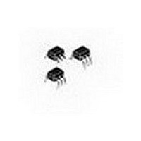
CNY171SR2M Fairchild Semiconductor, CNY171SR2M Datasheet - Page 2

CNY171SR2M
Manufacturer Part Number
CNY171SR2M
Description
Transistor Output Optocouplers Optocoupler Hi Bvceo Phototransistor
Manufacturer
Fairchild Semiconductor
Specifications of CNY171SR2M
Input Type
DC
Output Type
DC
Output Device
Transistor With Base
Number Of Elements
1
Reverse Breakdown Voltage
6V
Forward Voltage
1.65V
Forward Current
60mA
Collector-emitter Voltage
70V
Package Type
PDIP W SMD
Isolation Voltage
5250Vrms
Power Dissipation
250mW
Collector-emitter Saturation Voltage
0.4V
Current Transfer Ratio
80%
Fall Time
20000ns
Rise Time
4000ns
Pin Count
6
Mounting
Surface Mount
Operating Temp Range
-55C to 100C
Operating Temperature Classification
Industrial
Configuration
1 Channel
Maximum Collector Emitter Voltage
70 V
Maximum Collector Emitter Saturation Voltage
0.4 V
Maximum Forward Diode Voltage
1.65 V
Maximum Power Dissipation
250 mW
Maximum Operating Temperature
+ 100 C
Minimum Operating Temperature
- 55 C
Package / Case
PDIP-6 Gull Wing
Maximum Fall Time
20 us
Maximum Input Diode Current
60 mA
Maximum Reverse Diode Voltage
6 V
Maximum Rise Time
4 us
Lead Free Status / RoHS Status
Compliant
CNY17-1, CNY17-3, CNY17-2, CNY17-4 Rev. 1.0.2
Electrical Characteristics
Individual Component Characteristics
Parameters
TOTAL DEVICE
Storage Temperature
Operating Temperature
Lead Solder Temperature
Total Device Power Dissipation @ 25°C (LED plus detector)
Derate Linearly From 25°C
EMITTER
Continuous Forward Current
Reverse Voltage
Forward Current - Peak (1 µs pulse, 300 pps)
LED Power Dissipation 25°C Ambient
Derate Linearly From 25°C
DETECTOR
Detector Power Dissipation @ 25°C
Derate Linearly from 25°C
Parameters
EMITTER
Input Forward Voltage
Capacitance
Reverse Leakage Current V
DETECTOR
Breakdown Voltage
Leakage Current
Capacitance
Collector to Emitter
Collector to Base
Emitter to Collector
Collector to Emitter
Collector to Base
Collector to Emitter
Collector to Base
Emitter to Base
I
I
V
I
I
I
V
V
V
V
V
F
F
C
C
E
F
R
CE
CB
CE
CB
EB
= 60 mA
= 10 mA
= 100 µA, I
= 1.0 mA, I
= 10 µA, I
= 0 V, f = 1.0 MHz
= 6 V
Test Conditions
= 10 V, I
= 10 V, I
= 0, f = 1 MHz
= 0, f = 1 MHz
= 0, f = 1 MHz
F
(T
F
F
F
F
= 0
= 0
= 0
A
= 0
= 0
= 25°C Unless otherwise specified.)
Symbol
BV
BV
BV
I
I
C
C
C
CEO
CBO
V
C
I
CEO
CBO
ECO
R
CE
CB
EB
2
F
J
Symbol
I
T
T
T
F
P
V
P
P
OPR
STG
SOL
I
(pk)
F
D
R
D
D
Device
non -M
non -M
-M
-M
All
All
All
All
All
All
All
All
All
Device
non -M
non -M
non -M
non -M
non -M
non -M
non -M
non -M
All
All
All
-M
-M
-M
All
-M
-M
-M
-M
-M
Min
70
70
7
260 for 10 sec
-55 to +150
-55 to +100
0.001
Typ
1.35
1.15
100
120
50
Value
18
10
20
10
1
8
2.94
3.50
1.41
1.76
2.67
250
260
120
135
150
200
1.5
3.0
1.8
60
90
6
Max
1.65
1.50
10
50
20
www.fairchildsemi.com
Units
mW/°C
mW/°C
mW/°C
mW
mW
mW
mA
°C
°C
°C
V
A
Units
µA
nA
nA
pF
pF
pF
pF
V
V
V
V


