FXL2T245L10X_NL Fairchild Semiconductor, FXL2T245L10X_NL Datasheet - Page 2
FXL2T245L10X_NL
Manufacturer Part Number
FXL2T245L10X_NL
Description
Manufacturer
Fairchild Semiconductor
Datasheet
1.FXL2T245L10X_NL.pdf
(9 pages)
Specifications of FXL2T245L10X_NL
Logic Family
FXL
Logical Function
Translator
Technology
CMOS
High Level Output Current
-24mA
Low Level Output Current
24mA
Operating Supply Voltage (typ)
1.8/2.5/3.3V
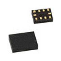
Package Type
MicroPak W
Operating Supply Voltage (max)
3.6V
Operating Supply Voltage (min)
1.1V
Abs. Propagation Delay Time
24ns
Mounting
Surface Mount
Pin Count
10
Operating Temperature (min)
-40C
Operating Temperature (max)
85C
Operating Temperature Classification
Industrial
Output Type
3-State
Lead Free Status / RoHS Status
Compliant


www.fairchildsemi.com
Pin Descriptions
Connection Diagram
Power-Up/Power-Down Sequencing
FXL translators offer an advantage in that either V
be powered up first. This benefit derives from the chip
design. When either V
HIGH-Impedance state. The control inputs (T/R and OE)
are designed to track the V
tying OE to V
tention, excessive currents, or oscillations do not occur
during power-up/power-down. The size of the pull-up resis-
tor is based upon the current-sinking capability of the OE
driver.
OE
T/R
A
B
V
V
GND
n
n
CCA
CCB
Pin Names
Pin Assignments for MicroPak
CCA
Output Enable Input
Transmit/Receive Input
Side A Inputs or 3-STATE Outputs
Side B Inputs or 3-STATE Outputs
Side A Power Supply
Side B Power Supply
Ground
should be used to ensure that bus con-
CC
(Top View)
is at 0 volts, outputs are in a
CCA
Description
supply. A pull-up resistor
CC
may
2
Truth Table
H
L
X
Pin Assignment
The recommended power-up sequence is the following:
1. Apply power to either V
2. Apply power to the T/R input (Logic HIGH for A-to-B
3. Apply power to other V
4. Drive the OE input LOW to enable the device.
The recommended power-down sequence is the following:
1. Drive OE input HIGH to disable the device.
2. Remove power from either V
3. Remove power from other V
LOW Voltage Level
HIGH Voltage Level
Don’t Care
operation; Logic LOW for B-to-A operation) and to the
respective data inputs (A Port or B Port). This may
occur at the same time as Step 1.
OE
L
L
Inputs
Pin Number
10
1
2
3
4
5
6
7
8
9
T/R
H
L
CC
CC
.
Bus B Data to Bus A
Bus A Data to Bus B
.
CC
CC
Terminal Name
.
.
V
V
GND
GND
Outputs
T/R
OE
CCA
A
A
B
B
CCB
0
1
1
0
Related parts for FXL2T245L10X_NL
Image
Part Number
Description
Manufacturer
Datasheet
Request
R

Part Number:
Description:
Fxl2t245 Low Voltage Dual Supply 2-bit Signal Translator With Configurable Voltage Supplies And Signal Levels And 3-state Outputs
Manufacturer:
Fairchild Semiconductor
Datasheet:
Part Number:
Description:
Fairchild Semiconductor [IGBT MODULE]
Manufacturer:
Fairchild Semiconductor
Datasheet:

Part Number:
Description:
Discrete Semiconductor Modules
Manufacturer:
Fairchild Semiconductor
Part Number:
Description:
Discrete Semiconductor Modules
Manufacturer:
Fairchild Semiconductor
Part Number:
Description:
This N-Channel MOSFET is produced using Fairchild Semiconductor’s advanced Power Trench® process
Manufacturer:
Fairchild Semiconductor
Datasheet:
Part Number:
Description:
This N-Channel MOSFET is produced using Fairchild Semiconductor’s advanced Power Trench® process
Manufacturer:
Fairchild Semiconductor
Datasheet:
Part Number:
Description:
This N-Channel MOSFET is produced using Fairchild Semiconductor’s advanced PowerTrench® process
Manufacturer:
Fairchild Semiconductor
Datasheet:
Part Number:
Description:
This N-Channel MOSFET is produced using Fairchild Semiconductor’s advanced PowerTrench® process
Manufacturer:
Fairchild Semiconductor
Datasheet:
Part Number:
Description:
This N-Channel MOSFET is produced using Fairchild Semiconductor’s advanced Power Trench® process
Manufacturer:
Fairchild Semiconductor
Datasheet:
Part Number:
Description:
This N-Channel logic Level MOSFETs are produced using Fairchild Semiconductor‘s advanced Power Trench® process that has been special tailored to minimize the on-state resistance and yet maintain superior switching performance
Manufacturer:
Fairchild Semiconductor
Datasheet:
Part Number:
Description:
This N-Channel MOSFET is produced using Fairchild Semiconductor’s advanced Power Trench® process
Manufacturer:
Fairchild Semiconductor
Datasheet:
Part Number:
Description:
This N-Channel SyncFET™ is produced using Fairchild Semiconductor’s advanced PowerTrench® process
Manufacturer:
Fairchild Semiconductor
Datasheet:
Part Number:
Description:
This N-Channel SyncFET™ is produced using Fairchild Semiconductor’s advanced PowerTrench® process
Manufacturer:
Fairchild Semiconductor
Datasheet:
Part Number:
Description:
This N-Channel SyncFET™ is produced using Fairchild Semiconductor’s advanced PowerTrench® process
Manufacturer:
Fairchild Semiconductor
Datasheet:
Part Number:
Description:
This N-Channel logic Level MOSFETs are produced using Fairchild Semiconductor‘s advanced Power Trench® process that has been special tailored to minimize the on-state resistance and yet maintain superior switching performance
Manufacturer:
Fairchild Semiconductor
Datasheet: