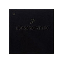
DSP56301VF100 Freescale, DSP56301VF100 Datasheet - Page 95

DSP56301VF100
Manufacturer Part Number
DSP56301VF100
Description
Manufacturer
Freescale
Datasheet
1.DSP56301VF100.pdf
(124 pages)
Specifications of DSP56301VF100
Device Core Size
24b
Format
Fixed Point
Clock Freq (max)
100MHz
Mips
100
Device Input Clock Speed
100MHz
Ram Size
24KB
Operating Supply Voltage (typ)
3.3V
Operating Supply Voltage (min)
3V
Operating Supply Voltage (max)
3.6V
Operating Temp Range
-40C to 100C
Operating Temperature Classification
Industrial
Mounting
Surface Mount
Pin Count
252
Package Type
MA-BGA
Lead Free Status / RoHS Status
Not Compliant
Available stocks
Company
Part Number
Manufacturer
Quantity
Price
Company:
Part Number:
DSP56301VF100
Manufacturer:
Freescale Semiconductor
Quantity:
10 000
Part Number:
DSP56301VF100
Manufacturer:
MOTOROLA/摩托罗拉
Quantity:
20 000
Freescale Semiconductor
Notes:
R10
R11
R12
Pin
No.
R4
R5
R6
R7
R8
R9
1.
2.
Signal names are based on configured functionality. Most connections supply a single signal. Some connections provide a
signal with dual functionality, such as the MODx/IRQx pins that select an operating mode after RESET is deasserted, but act as
interrupt lines during operation. Some signals have configurable polarity; these names are shown with and without overbars,
such as HAS/HAS. Some connections have two or more configurable functions; names assigned to these connections indicate
the function for a specific configuration. For example, connection N2 is data line H7 in non-multiplexed bus mode, data/address
line HAD7 in multiplexed bus mode, or GPIO line PB7 when the GPIO function is enabled for this pin. Unlike the TQFP
package, most of the GND pins are connected internally in the center of the connection array and act as heat sink for the chip.
Therefore, except for GND
chip.
NC stands for Not Connected. The following pin groups are shorted to each other:
— pins A2, B1, and B2
— pins A15, B15, B16, C14, C15, C16, and D14
— pins N3, R1, R2, and T2
— pins N16, P13, P15, R15, R16, and T15
Do not connect any line, component, trace, or via to these pins.
Table 3-3.
Signal Name
AA2/RAS2
BCLK
V
XTAL
CAS
BB
A3
A6
A9
CCP
DSP56301 MAP-BGA Signal Identification by Pin Number (Continued)
P
and GND
No.
R13
R14
R15
R16
Pin
T2
T3
T4
T5
T6
DSP56301 Technical Data, Rev. 10
P1
that support the PLL, other GND signals do not support individual subsystems in the
Signal Name
RESET
GND
PCAP
BCLK
A11
A14
NC
NC
NC
P1
No.
Pin
T10
T11
T12
T13
T14
T15
T7
T8
T9
MAP-BGA Package Description
Signal Name
A10
A13
WR
BR
RD
NC
A0
A4
A7
3-17


