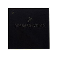
DSP56301VF100 Freescale, DSP56301VF100 Datasheet - Page 84

DSP56301VF100
Manufacturer Part Number
DSP56301VF100
Description
Manufacturer
Freescale
Datasheet
1.DSP56301VF100.pdf
(124 pages)
Specifications of DSP56301VF100
Device Core Size
24b
Format
Fixed Point
Clock Freq (max)
100MHz
Mips
100
Device Input Clock Speed
100MHz
Ram Size
24KB
Operating Supply Voltage (typ)
3.3V
Operating Supply Voltage (min)
3V
Operating Supply Voltage (max)
3.6V
Operating Temp Range
-40C to 100C
Operating Temperature Classification
Industrial
Mounting
Surface Mount
Pin Count
252
Package Type
MA-BGA
Lead Free Status / RoHS Status
Not Compliant
Available stocks
Company
Part Number
Manufacturer
Quantity
Price
Company:
Part Number:
DSP56301VF100
Manufacturer:
Freescale Semiconductor
Quantity:
10 000
Part Number:
DSP56301VF100
Manufacturer:
MOTOROLA/摩托罗拉
Quantity:
20 000
Packaging
3-6
Notes:
Pin
No.
151
152
153
154
155
156
157
158
159
160
161
162
163
164
165
166
167
168
169
170
1.
2.
HC0/HBE0, HA0, or PB16
Signal names are based on configured functionality. Most pins supply a single signal. Some pins provide a signal with dual
functionality, such as the MODx/IRQx pins that select an operating mode after RESET is deasserted, but act as interrupt lines
during operation. Some pins have two or more configurable functions; names assigned to these pins indicate the function for a
specific configuration. For example, Pin 165 is address/data line HAD6 in PCI bus mode, address line HA9 in non-PCI bus
mode, or GPIO line PB6 when the GPIO function is enabled for this pin.
NC stands for Not Connected. These pins are reserved for future development. Do not connect any line, component, trace, or
via to these pins.
HAD15, HD7, or PB15
HAD14, HD6, or PB14
HAD13, HD5, or PB13
HAD12, HD4, or PB12
HAD11, HD3, or PB11
HAD10, HD2, or PB10
HAD7, HA10, or PB7
HAD9, HD1, or PB9
HAD8, HD0, or PB8
HAD6, HA9, or PB6
HAD5, HA8, or PB5
HAD4, HA7, or PB4
HAD3, HA6, or PB3
Signal Name
Table 3-1.
GND
GND
V
V
NC
NC
CCH
CCH
H
H
DSP56301 TQFP Signal Identification by Pin Number (Continued)
No.
Pin
171
172
173
174
175
176
177
178
179
180
181
182
183
184
185
186
187
188
189
190
DSP56301 Technical Data, Rev. 10
HAD2, HA5, or PB2
HAD1, HA4, or PB1
HAD0, HA3, or PB0
Signal Name
SRD1 or PD4
SCLK or PE2
SC12 or PD2
SC11 or PD1
SC10 or PD0
STD1 or PD5
SCK1 or PD3
RXD or PE0
TXD or PE1
HINTA
GND
GND
V
V
TIO2
TIO1
TIO0
CCQ
CCS
S
Q
No.
Pin
191
192
193
194
195
196
197
198
199
200
201
202
203
204
205
206
207
208
Freescale Semiconductor
Signal Name
SRD0 or PC4
SCK0 or PC3
STD0 or PC5
SC00 or PC0
SC01 or PC1
SC02 or PC2
GND
TRST
V
TMS
TCK
TDO
TDI
DE
NC
NC
BS
BL
CCS
S


