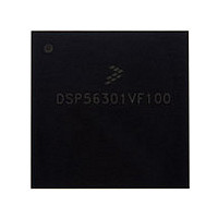
DSP56301VF100 Freescale, DSP56301VF100 Datasheet - Page 59

DSP56301VF100
Manufacturer Part Number
DSP56301VF100
Description
Manufacturer
Freescale
Datasheet
1.DSP56301VF100.pdf
(124 pages)
Specifications of DSP56301VF100
Device Core Size
24b
Format
Fixed Point
Clock Freq (max)
100MHz
Mips
100
Device Input Clock Speed
100MHz
Ram Size
24KB
Operating Supply Voltage (typ)
3.3V
Operating Supply Voltage (min)
3V
Operating Supply Voltage (max)
3.6V
Operating Temp Range
-40C to 100C
Operating Temperature Classification
Industrial
Mounting
Surface Mount
Pin Count
252
Package Type
MA-BGA
Lead Free Status / RoHS Status
Not Compliant
Available stocks
Company
Part Number
Manufacturer
Quantity
Price
Company:
Part Number:
DSP56301VF100
Manufacturer:
Freescale Semiconductor
Quantity:
10 000
Part Number:
DSP56301VF100
Manufacturer:
MOTOROLA/摩托罗拉
Quantity:
20 000
The asynchronous bus arbitration is enabled by internal
synchronization circuits add delay from the external signal until it is exposed to internal logic. As a result of this
delay, a DSP56300 part can assume mastership and assert
defines when
Once
DSP56300 components which are potential masters on the same bus. If
situation of
same time. Therefore, a non-overlap period between one
Timing 251 ensures that such a situation is avoided.
2.5.6
Freescale Semiconductor
No.
300
301
302
303
304
305
306
307
308
309
310
311
312
BB
Access Cycle Time
HA[10–0], HAEN Setup to Data Strobe Assertion
HA[10–0], HAEN Valid Hold from Data Strobe Deassertion
HRW Setup to HDS Assertion
HRW Valid Hold from HDS Deassertion
Data Strobe Deasserted Width
Data Strobe Asserted Pulse Width
HBS Asserted Pulse Width
HBS Assertion to Data Strobe Assertion
HBS Assertion to Data Strobe Deassertion
HBS Deassertion to Data Strobe Deassertion
Data Out Valid to TA Assertion (HBS Not Used—Tied to V
Data Out Active from Read Data Strobe Assertion
is asserted, there is a synchronization delay from
BG
Host Interface Timing
BB
asserted, and
can be asserted.
BG1
BB
BG2
Characteristic
BB
Table 2-18.
2
1
Figure 2-26.
deasserted, can cause another DSP56300 component to assume mastership at the
1
2
1
1
DSP56301 Technical Data, Rev. 10
1
Universal Bus Mode Timing Parameters
1
3
Asynchronous Bus Arbitration Timing
CC
1
)
2
BB
BG
BB
BB
250
inputs and synchronization circuits on
input active to another
, for some time after
assertion to the time this assertion is exposed to other
100 MHz: 2.5 × T
100 MHz: 2.5 × T
100 MHz: 1.5 × T
80 MHz: 2.5 × T
80 MHz: 2.5 × T
80 MHz: 1.5 × T
80 MHz: 2 × T
100 MHz: 2 × T
100 MHz: T
80 MHz: T
250+251
Expression
3 × T
BG
C
C
C
C
− 4.9
− 4.0
C
C
C
C
− 11.6
C
C
C
input is asserted before that time, a
251
− 9.2
+ 2.9
+ 3.3
+ 1.7
+ 1.3
+ 2.3
+ 2.6
BG
37.5
32.9
34.1
22.1
13.4
Min
BG
5.8
0.0
5.8
0.0
4.1
2.5
1.7
—
80 MHz
is deasserted. Timing 250
AC Electrical Characteristics
input active is required.
Max
7.6
—
—
—
—
—
—
—
—
—
—
—
—
Min
30.0
26.3
27.3
17.6
10.8
4.6
0.0
4.6
0.0
3.3
2.0
1.3
BG
—
100 MHz
. These
Max
6.0
—
—
—
—
—
—
—
—
—
—
—
—
Unit
2-33
ns
ns
ns
ns
ns
ns
ns
ns
ns
ns
ns
ns
ns
ns
ns
ns
ns
ns


