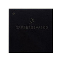
DSP56301VF100 Freescale, DSP56301VF100 Datasheet - Page 62

DSP56301VF100
Manufacturer Part Number
DSP56301VF100
Description
Manufacturer
Freescale
Datasheet
1.DSP56301VF100.pdf
(124 pages)
Specifications of DSP56301VF100
Device Core Size
24b
Format
Fixed Point
Clock Freq (max)
100MHz
Mips
100
Device Input Clock Speed
100MHz
Ram Size
24KB
Operating Supply Voltage (typ)
3.3V
Operating Supply Voltage (min)
3V
Operating Supply Voltage (max)
3.6V
Operating Temp Range
-40C to 100C
Operating Temperature Classification
Industrial
Mounting
Surface Mount
Pin Count
252
Package Type
MA-BGA
Lead Free Status / RoHS Status
Not Compliant
Available stocks
Company
Part Number
Manufacturer
Quantity
Price
Company:
Part Number:
DSP56301VF100
Manufacturer:
Freescale Semiconductor
Quantity:
10 000
Part Number:
DSP56301VF100
Manufacturer:
MOTOROLA/摩托罗拉
Quantity:
20 000
Specifications
2-36
330
331
332
346
347
348
Notes:
No.
HIRQ High Impedance from Data Strobe Assertion
(HIRH = 1, HIRD = 0)
HIRQ Active from Data Strobe Deassertion
(HIRH = 1, HIRD = 0)
HIRQ Deasserted Hold from Data Strobe Deassertion
HRST Assertion to Host Port Pins High Impedance
HBS Assertion to CLKOUT Rising Edge
Data Strobe Deassertion to CLKOUT Rising Edge
1.
2.
3.
4.
5.
6.
7.
8.
The Data Strobe is HRD or HWR in the Dual Data Strobe mode and HDS in the Single Data Strobe mode.
HTA, HDRQ, and HRST may be programmed as active-high or active-low. In the example timing diagrams, HDRQ and HRST
are shown as active-high and HTA is shown as active low.
The Read Data Strobe is HRD in the Dual Data Strobe mode and HDS in the Single Data Strobe mode.
The Write Data Strobe is HWR in the Dual Data Strobe mode and HDS in the Single Data Strobe mode.
HTA requires an external pull-down resistor if programmed as active high (HTAP = 0); or an external pull-up resistor if
programmed as active low (HTAP = 1). The resistor value should be consistent with the DC specifications.
HIRQ requires an external pull-up resistor if programmed as open drain (HIRD = 0). The resistor value should be consistent
with the DC specifications.
“LT” is the value of the latency timer register (CLAT) as programmed by the user during self configuration.
Values are valid for V
Table 2-19.
(HIRD = 1,
(HIRD = 0,
HIRH = 1)
HIRH = 1)
HA[10–0]
HDS
HRD
HWR
HIRQ
HIRQ
HBS
1,6
1
Characteristic
Universal Bus Mode, Synchronous Port A Type Host Timing (Continued)
Figure 2-27.
CC
= 3.3 ± 0.3V
DSP56301 Technical Data, Rev. 10
305
308
Universal Bus Mode I/O Access Timing
301
1
2
307
1
329
330
309
100 MHz: 2.5 × T
80 MHz: 2.5 × T
328
Expression
2.5 × T
2.5 × T
310
C
C
C
C
+ 24.7
+ 21.5
31.3
31.3
Min
4.3
7.4
—
—
80 MHz
302
332
331
Max
55.9
22.2
—
—
—
—
Freescale Semiconductor
Min
25.0
25.0
3.4
5.9
—
—
100 MHz
Max
46.5
19.6
—
—
—
—
Unit
ns
ns
ns
ns
ns
ns
ns


