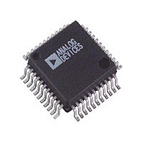
ADV7176AKS Analog Devices Inc, ADV7176AKS Datasheet - Page 13

ADV7176AKS
Manufacturer Part Number
ADV7176AKS
Description
Manufacturer
Analog Devices Inc
Datasheet
1.ADV7176AKS.pdf
(50 pages)
Specifications of ADV7176AKS
Adc/dac Resolution
10b
Screening Level
Commercial
Package Type
MQFP
Pin Count
44
Lead Free Status / RoHS Status
Not Compliant
Available stocks
Company
Part Number
Manufacturer
Quantity
Price
Company:
Part Number:
ADV7176AKS
Manufacturer:
AD
Quantity:
5 510
Company:
Part Number:
ADV7176AKS
Manufacturer:
VIS
Quantity:
5 510
Company:
Part Number:
ADV7176AKS
Manufacturer:
AD
Quantity:
513
Part Number:
ADV7176AKSZ
Manufacturer:
ADI/亚德诺
Quantity:
20 000
COLOR BAR GENERATION
The ADV7175A/ADV7176A can be configured to generate
100/7.5/75/7.5 for NTSC color bars or 100/0/75/0 for PAL
color bars. These are enabled by setting MR17 of Mode Reg-
ister 1 to Logic “1.”
SQUARE PIXEL MODE
The ADV7175A/ADV7176A can be used to operate in square
pixel mode. For NTSC operation an input clock of 24.5454 MHz
is required. Alternatively an input clock of 29.5 MHz is required
for PAL operation. The internal timing logic adjusts accordingly
for square pixel mode operation.
COLOR SIGNAL CONTROL
The color information can be switched on and off the video
output using Bit MR24 of Mode Register 2.
BURST SIGNAL CONTROL
The burst information can be switched on and off the video
output using Bit MR25 of Mode Register 2.
NTSC PEDESTAL CONTROL
The pedestal on both odd and even fields can be controlled on a
line-by-line basis using the NTSC Pedestal Control Registers.
This allows the pedestals to be controlled during the vertical
blanking interval (Lines 10 to 25 and Lines 273 to 288).
PIXEL TIMING DESCRIPTION
The ADV7175A/ADV7176A can operate in either 8-bit or
16-bit YCrCb Mode.
8-Bit YCrCb Mode
This default mode accepts multiplexed YCrCb inputs through
the P7-P0 pixel inputs. The inputs follow the sequence Cb0, Y0
Cr0, Y1 Cb1, Y2, etc. The Y, Cb and Cr data are input on a
rising clock edge.
16-Bit YCrCb Mode
This mode accepts Y inputs through the P7–P0 pixel inputs and
multiplexed CrCb inputs through the P15–P8 pixel inputs. The
data is loaded on every second rising edge of CLOCK. The inputs
follow the sequence Cb0, Y0 Cr0, Y1 Cb1, Y2, etc.
–10
–20
–30
–40
–50
–60
0
0
2
4
FREQUENCY – MHz
6
8
10
12
SUBCARRIER RESET
Together with the SCRESET/RTC PIN and Bits MR22 and
MR21 of Mode Register 2, the ADV7175A/ADV7176A can be
used in subcarrier reset mode. The subcarrier will reset to
Field 0 at the start of the following field when a low to high
transition occurs on this input pin.
REAL TIME CONTROL
Together with the SCRESET/RTC PIN and Bits MR22 and
MR21 of Mode Register 2, the ADV7175A/ADV7176A can be
used to lock to an external video source. The real time control
mode allows the ADV7175A/ADV7176A to automatically alter
the subcarrier frequency to compensate for line length variation.
When the part is connected to a device that outputs a digital
datastream in the RTC format (such as an ADV7185 video
decoder [see Figure 13]), the part will automatically change to
the compensated subcarrier frequency on a line by line basis.
This digital datastream is 67 bits wide and the subcarrier is
contained in Bits 0 to 21. Each bit is two clock cycles long.
00HEX should be written to all four subcarrier frequency regis-
ters when using this mode.
VIDEO TIMING DESCRIPTION
The ADV7175A/ADV7176A is intended to interface to off-
the-shelf MPEG1 and MPEG2 Decoders. Consequently, the
ADV7175A/ADV7176A accepts 4:2:2 YCrCb Pixel Data via a
CCIR-656 pixel port and has several video timing modes of
operation that allow it to be configured as either system master
video timing generator or a slave to the system video timing
generator. The ADV7175A/ADV7176A generates all of the
required horizontal and vertical timing periods and levels for the
analog video outputs.
The ADV7175A/ADV7176A calculates the width and place-
ment of analog sync pulses, blanking levels and color burst
envelopes. Color bursts are disabled on appropriate lines, and
serration and equalization pulses are inserted where required.
In addition the ADV7175A/ADV7176A supports a PAL or
NTSC square pixel operation in slave mode. The part requires
an input pixel clock of 24.5454 MHz for NTSC and an input
pixel clock of 29.5 MHz for PAL. The internal horizontal line
counters place the various video waveform sections in the cor-
rect location for the new clock frequencies.
The ADV7175A/ADV7176A has four distinct master and four
distinct slave timing configurations. Timing Control is estab-
lished with the bidirectional SYNC, BLANK and FIELD/
VSYNC pins. Timing Mode Register 1 can also be used to vary
the timing pulsewidths and where they occur in relation to
each other.
ADV7175A/ADV7176A


