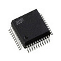
SAA7103HV4 NXP Semiconductors, SAA7103HV4 Datasheet - Page 13

SAA7103HV4
Manufacturer Part Number
SAA7103HV4
Description
Manufacturer
NXP Semiconductors
Datasheet
1.SAA7103HV4.pdf
(84 pages)
Specifications of SAA7103HV4
Adc/dac Resolution
10b
Screening Level
Commercial
Package Type
PQFP
Pin Count
44
Lead Free Status / RoHS Status
Compliant
Philips Semiconductors
SAA7102_SAA7103_4
Product data sheet
7.12.2 Teletext insertion and encoding (not simultaneously with real-time control)
7.12.3 Video Programming System (VPS) encoding
7.12.4 Closed caption encoder
schemes. Other manipulations used for the Macrovision anti-taping process, such as
additional insertion of AGC super-white pulses (programmable in height), are supported
by the SAA7102 only.
To enable easy analog post filtering, luminance is interpolated from a 13.5 MHz data rate
to a 27 MHz data rate, thereby providing luminance in a 10-bit resolution. The transfer
characteristics of the luminance interpolation filter are illustrated in
Appropriate transients at start/end of active video and for synchronization pulses are
ensured.
Chrominance is modified in gain (programmable separately for C
standard dependent burst is inserted, before baseband color signals are interpolated from
a 6.75 MHz data rate to a 27 MHz data rate. One of the interpolation stages can be
bypassed, thus providing a higher color bandwidth, which can be used for the Y and C
output. The transfer characteristics of the chrominance interpolation filter are illustrated in
Figure 6
The amplitude (beginning and ending) of the inserted burst, is programmable in a certain
range that is suitable for standard signals and for special effects. After the succeeding
quadrature modulator, color is provided on the subcarrier in 10-bit resolution.
The numeric ratio between the Y and C outputs is in accordance with the standards.
Pin TTX_SRES receives a WST or NABTS teletext bitstream sampled at the crystal clock.
At each rising edge of the output signal (TTXRQ) a single teletext bit has to be provided
after a programmable delay at input pin TTX_SRES.
Phase variant interpolation is achieved on this bitstream in the internal teletext encoder,
providing sufficient small phase jitter on the output text lines.
TTXRQ_XCLKO2 provides a fully programmable request signal to the teletext source,
indicating the insertion period of bitstream at lines which can be selected independently
for both fields. The internal insertion window for text is set to 360 (PAL WST),
296 (NTSC WST) or 288 (NABTS) teletext bits including clock run-in bits. The protocol
and timing are illustrated in
Alternatively, this pin can be provided with a buffered crystal clock (XCLK) of 13.5 MHz.
Five bytes of VPS information can be loaded via the I
appropriate format into line 16.
Using this circuit, data in accordance with the specification of closed caption or extended
data service, delivered by the control interface, can be encoded (line 21). Two dedicated
pairs of bytes (two bytes per field), each pair preceded by run-in clocks and framing code,
are possible.
The actual line number in which data is to be encoded, can be modified in a certain range.
The data clock frequency is in accordance with the definition for NTSC M standard
32 times horizontal line frequency.
and
Figure
7.
Rev. 04 — 18 January 2006
Figure
15.
SAA7102; SAA7103
2
C-bus and will be encoded in the
© Koninklijke Philips Electronics N.V. 2006. All rights reserved.
B
and C
Digital video encoder
Figure 8
R
), and a
and
Figure
13 of 84
9.


