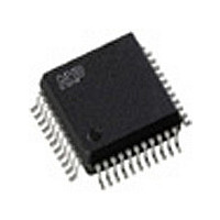
SAA7103HV4 NXP Semiconductors, SAA7103HV4 Datasheet - Page 12

SAA7103HV4
Manufacturer Part Number
SAA7103HV4
Description
Manufacturer
NXP Semiconductors
Datasheet
1.SAA7103HV4.pdf
(84 pages)
Specifications of SAA7103HV4
Adc/dac Resolution
10b
Screening Level
Commercial
Package Type
PQFP
Pin Count
44
Lead Free Status / RoHS Status
Compliant
Philips Semiconductors
SAA7102_SAA7103_4
Product data sheet
7.12.1 Video path
7.10 Oscillator and Discrete Time Oscillator (DTO)
7.11 Low-pass Clock Generation Circuit (CGC)
7.12 Encoder
7.8 FIFO
7.9 Border generator
Due to the re-interlacing, the circuit can perform upscaling. The maximum factor depends
on the setting of the anti-flicker function and can be derived from the formulae given in
Section
The FIFO acts as a buffer to translate from the PIXCLK clock domain to the XTAL clock
domain. The write clock is PIXCLK and the read clock is XTAL. An underflow or overflow
condition can be detected via the I
In order to avoid underflows and overflows, it is essential that the frequency of the
synthesized PIXCLK matches to the input graphics resolution and the desired scaling
factor. It is suggested to refer to
When the graphics picture is to be displayed as interlaced PAL, NTSC, S-video or RGB on
a TV screen, it is desired in many cases not to lose picture information due to the inherent
overscanning of a TV set. The desired amount of underscan area, which is achieved
through appropriate scaling in the vertical and horizontal direction, can be filled in the
border generator with an arbitrary true color tint.
The master clock generation is realized as a 27 MHz crystal oscillator, which can operate
with either a fundamental wave crystal or a 3rd-harmonic crystal.
The crystal clock supplies the DTO of the pixel clock synthesizer, the video encoder and
the I
auxiliary VGA mode, where the triple DAC is clocked by the pixel clock (PIXCLK).
The DTO can be programmed to synthesize all relevant pixel clock frequencies between
circa 18 MHz and 44 MHz.
This block reduces the phase jitter of the synthesized pixel clock. It works as a tracking
filter for all relevant synthesized pixel clock frequencies.
The encoder generates luminance and color subcarrier output signals from the Y,
C
signals.
Input to the encoder, at 27 MHz clock (e.g. DVD), is either originated from computer
graphics at pixel clock, fed through the FIFO and border generator, or a ITU-R BT.656
style signal.
Luminance is modified in gain and in offset (the offset is programmable in a certain range
to enable different black level set-ups). A blanking level can be set after insertion of a fixed
synchronization pulse tip level, in accordance with standard composite synchronization
B
and C
2
C-bus control block. It also usually supplies the triple DAC, with the exception of the
7.17.
R
baseband signals, which are suitable for use as CVBS or separate Y and C
Rev. 04 — 18 January 2006
Table 9
2
C-bus read access.
to
Table 26
SAA7102; SAA7103
for some representative combinations.
© Koninklijke Philips Electronics N.V. 2006. All rights reserved.
Digital video encoder
12 of 84


