PIC24FJ64GA110-I/PT Microchip Technology, PIC24FJ64GA110-I/PT Datasheet - Page 324
PIC24FJ64GA110-I/PT
Manufacturer Part Number
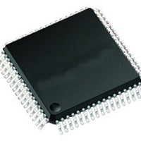
PIC24FJ64GA110-I/PT
Description
16-bit, 16 MIPS, 64KB Flash, 16Kb RAM, 84 I/O, NanoWatt 100 TQFP 12x12x1mm TRAY
Manufacturer
Microchip Technology
Series
PIC® 24Fr
Datasheet
1.PIC24FJ128GA106-IPT.pdf
(330 pages)
Specifications of PIC24FJ64GA110-I/PT
Core Processor
PIC
Core Size
16-Bit
Speed
32MHz
Connectivity
I²C, IrDA, LIN, SPI, UART/USART
Peripherals
Brown-out Detect/Reset, LVD, POR, PWM, WDT
Number Of I /o
85
Program Memory Size
64KB (22K x 24)
Program Memory Type
FLASH
Ram Size
16K x 8
Voltage - Supply (vcc/vdd)
2 V ~ 3.6 V
Data Converters
A/D 16x10b
Oscillator Type
Internal
Operating Temperature
-40°C ~ 85°C
Package / Case
100-TQFP
Processor Series
PIC24FJ256GA110
Core
PIC
Data Bus Width
16 bit
Data Ram Size
16 KB
Interface Type
UART, I2C, SPI
Maximum Clock Frequency
8 MHz
Number Of Timers
5
Operating Supply Voltage
3.6 V
Maximum Operating Temperature
- 40 C to + 85 C
Mounting Style
SMD/SMT
Lead Free Status / RoHS Status
Lead free / RoHS Compliant
Eeprom Size
-
Lead Free Status / Rohs Status
Details
Available stocks
Company
Part Number
Manufacturer
Quantity
Price
Company:

Part Number:
PIC24FJ64GA110-I/PT
Manufacturer:
Microchip Technology
Quantity:
10 000


PIC24FJ256GA110 FAMILY
DS39905E-page 324
IPC12 (Interrupt Priority Control 12) ........................ 103
IPC13 (Interrupt Priority Control 13) ........................ 104
IPC15 (Interrupt Priority Control 15) ........................ 105
IPC16 (Interrupt Priority Control 16) ........................ 106
IPC18 (Interrupt Priority Control 18) ........................ 107
IPC19 (Interrupt Priority Control 19) ........................ 107
IPC2 (Interrupt Priority Control 2) .............................. 93
IPC20 (Interrupt Priority Control 20) ........................ 108
IPC21 (Interrupt Priority Control 21) ........................ 109
IPC22 (Interrupt Priority Control 22) ........................ 110
IPC23 (Interrupt Priority Control 23) ........................ 111
IPC3 (Interrupt Priority Control 3) .............................. 94
IPC4 (Interrupt Priority Control 4) .............................. 95
IPC5 (Interrupt Priority Control 5) .............................. 96
IPC6 (Interrupt Priority Control 6) .............................. 97
IPC7 (Interrupt Priority Control 7) .............................. 98
IPC8 (Interrupt Priority Control 8) .............................. 99
IPC9 (Interrupt Priority Control 9) ............................ 100
MINSEC (RTCC Minutes and Seconds Value) ........ 217
MTHDY (RTCC Month and Day Value) ................... 216
NVMCON (Flash Memory Control) ............................ 59
OCxCON1 (Output Compare x Control 1) ............... 172
OCxCON2 (Output Compare x Control 2) ............... 173
OSCCON (Oscillator Control) .................................. 117
OSCTUN (FRC Oscillator Tune) .............................. 120
PADCFG1 (Pad Configuration Control) ........... 207, 214
PMADDR (PMP Address) ........................................ 205
PMAEN (PMP Enable) ............................................. 205
PMCON (PMP Control) ............................................ 202
PMMODE (PMP Mode) ............................................ 204
PMSTAT (PMP Status) ............................................ 206
RCFGCAL (RTCC Calibration and
RCON (Reset Control) ............................................... 66
REFOCON (Reference Oscillator Control) ............... 123
RPINR0 (Peripheral Pin Select Input 0) ................... 135
RPINR1 (Peripheral Pin Select Input 1) ................... 135
RPINR10 (Peripheral Pin Select Input 10) ............... 139
RPINR11 (Peripheral Pin Select Input 11) ............... 139
RPINR15 (Peripheral Pin Select Input 15) ............... 140
RPINR17 (Peripheral Pin Select Input 17) ............... 140
RPINR18 (Peripheral Pin Select Input 18) ............... 141
RPINR19 (Peripheral Pin Select Input 19) ............... 141
RPINR2 (Peripheral Pin Select Input 2) ................... 136
RPINR20 (Peripheral Pin Select Input 20) ............... 142
RPINR21 (Peripheral Pin Select Input 21) ............... 142
RPINR22 (Peripheral Pin Select Input 22) ............... 143
RPINR23 (Peripheral Pin Select Input 23) ............... 143
RPINR27 (Peripheral Pin Select Input 27) ............... 144
RPINR28 (Peripheral Pin Select Input 28) ............... 144
RPINR29 (Peripheral Pin Select Input 29) ............... 145
RPINR3 (Peripheral Pin Select Input 3) ................... 136
RPINR4 (Peripheral Pin Select Input 4) ................... 137
RPINR7 (Peripheral Pin Select Input 7) ................... 137
RPINR8 (Peripheral Pin Select Input 8) ................... 138
RPINR9 (Peripheral Pin Select Input 9) ................... 138
RPOR0 (PPS Output 0) ........................................... 146
RPOR1 (PPS Output 1) ........................................... 146
RPOR10 (PPS Output 10) ....................................... 151
RPOR11 (PPS Output 11) ....................................... 151
RPOR12 (PPS Output 12) ....................................... 152
RPOR13 (PPS Output 13) ....................................... 152
RPOR14 (PPS Output 14) ....................................... 153
RPOR15 (PPS Output 15) ....................................... 153
RPOR2 (PPS Output 2) ........................................... 147
Configuration) .................................................. 213
Registers Maps
Resets
Revision History ............................................................... 319
RTCC
S
Selective Peripheral Power Control ................................. 126
Serial Peripheral Interface. See SPI.
SFR Space ........................................................................ 38
Software Simulator (MPLAB SIM) ................................... 267
Software Stack ................................................................... 53
SPI
Symbols Used in Opcode Descriptions ........................... 258
T
Timer1 .............................................................................. 155
Timer2/3 and Timer4/5
Timing Diagrams
RPOR3 (PPS Output 3) ........................................... 147
RPOR4 (PPS Output 4) ........................................... 148
RPOR5 (PPS Output 5) ........................................... 148
RPOR6 (PPS Output 6) ........................................... 149
RPOR7 (PPS Output 7) ........................................... 149
RPOR8 (PPS Output 8) ........................................... 150
RPOR9 (PPS Output 9) ........................................... 150
SPIxCON1 (SPIx Control 1) ..................................... 180
SPIxCON2 (SPIx Control 2) ..................................... 181
SPIxSTAT (SPIx Status and Control) ...................... 178
SR (ALU STATUS, in CPU) ....................................... 75
SR (ALU STATUS) .................................................... 32
T1CON (Timer1 Control) ......................................... 156
TxCON (Timer2 and Timer4 Control) ...................... 160
TyCON (Timer3 and Timer5 Control) ...................... 161
UxMODE (UARTx Mode) ......................................... 196
UxSTA (UARTx Status and Control) ........................ 198
WKDYHR (RTCC Weekday and Hours Value) ........ 217
YEAR (RTCC Year Value) ....................................... 216
PORTG ...................................................................... 48
Clock Source Selection .............................................. 67
Delay Times ............................................................... 68
RCON Flag Operation ............................................... 67
SFR States ................................................................ 69
Alarm Configuration ................................................. 220
Calibration ............................................................... 219
Register Mapping ..................................................... 212
Baud Rate Generator Output ................................... 289
CLKO and I/O Characteristics ................................. 285
External Clock Requirements .................................. 283
I
I
I
I
Input Capture ........................................................... 290
Output Compare ...................................................... 295
Parallel Master Port Read ........................................ 301
Parallel Master Port Write ........................................ 302
PWM Requirements ................................................. 295
Reset, Watchdog Timer. Oscillator Start-up
SPIx Master Mode (CKE = 0) .................................. 291
SPIx Master Mode (CKE = 1) .................................. 292
SPIx Slave Mode (CKE = 0) .................................... 293
SPIx Slave Mode (CKE = 1) .................................... 294
Start Bit Edge Detection .......................................... 289
2
2
2
2
C Bus Data (Master Mode) ................................... 297
C Bus Data (Slave Mode) ..................................... 299
C Bus Start/Stop Bits (Master Mode) .................... 296
C Bus Start/Stop Bits (Slave Mode) ...................... 298
Timer, Power-up Timer Characteristics ..... 272, 288
2010 Microchip Technology Inc.
Related parts for PIC24FJ64GA110-I/PT
Image
Part Number
Description
Manufacturer
Datasheet
Request
R

Part Number:
Description:
Manufacturer:
Microchip Technology Inc.
Datasheet:
Part Number:
Description:
Manufacturer:
Microchip Technology Inc.
Datasheet:
Part Number:
Description:
Manufacturer:
Microchip Technology Inc.
Datasheet:
Part Number:
Description:
Manufacturer:
Microchip Technology Inc.
Datasheet:
Part Number:
Description:
Manufacturer:
Microchip Technology Inc.
Datasheet:
Part Number:
Description:
Manufacturer:
Microchip Technology Inc.
Datasheet:
Part Number:
Description:
Manufacturer:
Microchip Technology Inc.
Datasheet:
Part Number:
Description:
Manufacturer:
Microchip Technology Inc.
Datasheet: