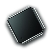
PIC18F87K90T-I/PT Microchip Technology, PIC18F87K90T-I/PT Datasheet - Page 52

PIC18F87K90T-I/PT
Manufacturer Part Number
PIC18F87K90T-I/PT
Description
128kB Flash, 4kB RAM, 1kB EE, 16MIPS, NanoWatt XLP, LCD, 5V 80 TQFP 12x12x1mm T/
Manufacturer
Microchip Technology
Series
PIC® XLP™ 18Fr
Datasheet
1.PIC18F66K90-IMR.pdf
(570 pages)
Specifications of PIC18F87K90T-I/PT
Processor Series
PIC18F
Core
PIC
Data Bus Width
8 bit
Program Memory Type
Flash
Program Memory Size
128 KB
Data Ram Size
4 KB
Interface Type
I2C, SPI
Maximum Clock Frequency
64 MHz
Number Of Timers
11
Operating Supply Voltage
1.8 V to 5.5 V
Maximum Operating Temperature
+ 125 C
3rd Party Development Tools
52715-96, 52716-328, 52717-734, 52712-325, EWPIC18
Minimum Operating Temperature
- 40 C
On-chip Adc
12 bit, 24 Channel
Core Processor
PIC
Core Size
8-Bit
Speed
64MHz
Connectivity
I²C, LIN, SPI, UART/USART
Peripherals
Brown-out Detect/Reset, LCD, POR, PWM, WDT
Number Of I /o
69
Eeprom Size
1K x 8
Ram Size
4K x 8
Voltage - Supply (vcc/vdd)
1.8 V ~ 5.5 V
Data Converters
A/D 24x12b
Oscillator Type
Internal
Operating Temperature
-40°C ~ 85°C
Package / Case
80-TQFP
Lead Free Status / Rohs Status
Details
Available stocks
Company
Part Number
Manufacturer
Quantity
Price
Company:
Part Number:
PIC18F87K90T-I/PT
Manufacturer:
Microchip Technology
Quantity:
10 000
Company:
Part Number:
PIC18F87K90T-I/PTRSL
Manufacturer:
Microchip Technology
Quantity:
10 000
- Current page: 52 of 570
- Download datasheet (5Mb)
PIC18F87K90 FAMILY
3.8
When PRI_IDLE mode is selected, the designated pri-
mary oscillator continues to run without interruption.
For all other power-managed modes, the oscillator
using the OSC1 pin is disabled. The OSC1 pin (and
OSC2 pin if used by the oscillator) will stop oscillating.
In
SEC_IDLE), the SOSC oscillator is operating and
providing the device clock. The SOSC oscillator may
also run in all power-managed modes if required to
clock SOSC.
In RC_RUN and RC_IDLE modes, the internal
oscillator provides the device clock source. The 31 kHz
LF-INTOSC output can be used directly to provide the
clock and may be enabled to support various special
features, regardless of the power-managed mode (see
Section 28.2 “Watchdog Timer (WDT)”
Section 28.5 “Fail-Safe Clock Monitor”
information on WDT, Fail-Safe Clock Monitor and
Two-Speed Start-up).
If the Sleep mode is selected, all clock sources are
stopped. Since all the transistor switching currents
have been stopped, Sleep mode achieves the lowest
current consumption of the device (only leakage
currents).
Enabling any on-chip feature that will operate during
Sleep will increase the current consumed during Sleep.
The INTOSC is required to support WDT operation.
The SOSC oscillator may be operating to support a
TABLE 3-4:
DS39957D-page 52
EC, ECPLL
HS, HSPLL
INTOSC, INTPLL1/2
Note:
secondary
Oscillator Mode
Effects of Power-Managed Modes
on the Various Clock Sources
See
Section 5.0 “Reset”
OSC1 AND OSC2 PIN STATES IN SLEEP MODE
clock
modes
Floating, pulled by external clock
Feedback inverter is disabled at quiescent
voltage level
I/O pin, RA6, direction is controlled by
TRISA<6>
(SEC_RUN
for time-outs due to Sleep and MCLR Reset.
for more
OSC1 Pin
through
and
Real-Time Clock (RTC). Other features may be operat-
ing that do not require a device clock source (i.e.,
MSSP slave, INTx pins and others). Peripherals that
may add significant current consumption are listed in
Section 31.2 “DC Characteristics: Power-Down and
Supply Current PIC18F87K90 Family (Industrial/
Extended)”.
3.9
Power-up delays are controlled by two timers, so that
no external Reset circuitry is required for most applica-
tions. The delays ensure that the device is kept in
Reset until the device power supply is stable under nor-
mal circumstances and the primary clock is operating
and stable. For additional information on power-up
delays, see
The first timer is the Power-up Timer (PWRT), which
provides a fixed delay on a power-up time of about
64 ms (Parameter 33,
enabled.
The second timer is the Oscillator Start-up Timer
(OST), intended to keep the chip in Reset until the
crystal oscillator is stable (HS, XT or LP modes). The
OST does this by counting 1,024 oscillator cycles
before allowing the oscillator to clock the device.
There is a delay of interval, T
Table
becomes ready to execute instructions.
31-10), following POR, while the controller
Power-up Delays
At logic low (clock/4 output)
Feedback inverter is disabled at quiescent
voltage level
I/O pin, RA6, direction is controlled by
TRISA<7>
Section 5.6 “Power-up Timer
2009-2011 Microchip Technology Inc.
Table
OSC2 Pin
31-10); it is always
CSD
(Parameter 38,
(PWRT)”.
Related parts for PIC18F87K90T-I/PT
Image
Part Number
Description
Manufacturer
Datasheet
Request
R

Part Number:
Description:
Manufacturer:
Microchip Technology Inc.
Datasheet:

Part Number:
Description:
Manufacturer:
Microchip Technology Inc.
Datasheet:

Part Number:
Description:
Manufacturer:
Microchip Technology Inc.
Datasheet:

Part Number:
Description:
Manufacturer:
Microchip Technology Inc.
Datasheet:

Part Number:
Description:
Manufacturer:
Microchip Technology Inc.
Datasheet:

Part Number:
Description:
Manufacturer:
Microchip Technology Inc.
Datasheet:

Part Number:
Description:
Manufacturer:
Microchip Technology Inc.
Datasheet:

Part Number:
Description:
Manufacturer:
Microchip Technology Inc.
Datasheet:


