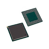
CYP15G0402DXB-BGI Cypress Semiconductor Corp, CYP15G0402DXB-BGI Datasheet - Page 9

CYP15G0402DXB-BGI
Manufacturer Part Number
CYP15G0402DXB-BGI
Description
Manufacturer
Cypress Semiconductor Corp
Datasheet
1.CYP15G0402DXB-BGI.pdf
(29 pages)
Specifications of CYP15G0402DXB-BGI
Lead Free Status / RoHS Status
Not Compliant
Document #: 38-02057 Rev. *G
Pin Descriptions
FRAMCHAR
RXCLKA±
RXCLKB±
RXCLKC±
RXCLKD±
RFMODE
Device Control Signals
PARCTL
REFCLK±
SPDSEL
Name
Three-level Select
Static Control Input
LVTTL Output Clock Receive Character Clock Output. These true and complement clocks are the Receive
Three-level Select
Static Control Input
Three-level Select
Static Control Input
Differential LVPECL
or single-ended
LVCMOS input clock
Three-level Select
Static Control Input
I/O Characteristics Signal Description
CYP(V)15G0402DXB Quad HOTLink II™ SERDES (continued)
[5]
[5]
[5]
[5]
,
,
Framing Character Select. Used to control the type of character used for framing the
received data streams.
When MID, the framer looks for both positive and negative disparity versions of the
eight-bit Comma character.
When HIGH, the framer looks for both positive and negative disparity versions of the
K28.5 character.
Configuring FRAMCHAR to LOW is reserved for component test.
interface clocks which are used to control timing of data output transfers. These clocks
are output continuously at either the dual-character rate (1/20
character rate (1/10
RXRATE.
Reframe Mode Select. Used to control the type of character framing used to adjust the
character boundaries (based on detection of one or more framing characters in the
received serial bit stream). This signal operates in conjunction with the type of framing
character selected.
When LOW, the Low-Latency Framer is selected. This will frame on each occurrence
of the selected framing character(s) in the received data stream. This mode of framing
stretches the recovered character clock for one or multiple cycles to align that clock with
the recovered data.
When MID, the Cypress-mode Multi-Byte parallel Framer is selected. This requires a
pair of the selected framing character(s), on identical 10-bit boundaries, within a span
of 50 bits, before the character boundaries are adjusted. The recovered character clock
remains in the same phase regardless of character offset.
When HIGH, the alternate mode Multi-Byte parallel Framer is selected. This requires
detection of the selected framing character(s) of the allowed disparities in the received
serial bit stream, on identical 10-bit boundaries, on four directly adjacent characters.
The recovered character clock remains in the same phase regardless of character
offset.
Parity Check/Generate Control. Used to control the different parity check and
generate functions.
When LOW, parity checking is disabled, and the RXOPx outputs are all disabled
(High-Z).
When MID, theTXDx[9:0] inputs are checked (along with TXOPx) for valid ODD parity,
and ODD parity is generated for the RXDx[9:0] outputs and presented on RXOPx.
When HIGH, parity checking and generation are enabled. The TXDx[9:0] inputs are
checked (along with TXOPx) for valid ODD parity, and ODD parity is generated for the
RXDx[9:0] and COMDETx outputs and presented on RXOPx. See Table 8 for details.
Reference Clock. This clock input is used as the timing reference for the transmit PLL.
It is also used as the centering frequency of the Range Controller block of the Receive
CDR PLLs. This input clock may also be selected to clock the transmit input interface.
When driven by a a single-ended LVCMOS or LVTTL clock source, connect the clock
source to either the true or complement REFCLK input and leave the alternate REFCLK
input open (floating). When driven by an LVPECL clock source, the clock must be a
differential clock, using both inputs.
When TXCKSEL = LOW, REFCLK is also used as the clock for the parallel transmit data
(input) interface.
Serial Rate Select. This input specifies the operating bit-rate range of both transmit and
receive PLLs. LOW = 195–400 MBaud, MID = 400–800 MBaud, HIGH =
800–1500 MBaud. When SPDSEL is LOW, setting TXRATE = HIGH (Half-rate
Reference Clock) is invalid.
th
the serial bit-rate) of the data being received, as selected by
CYP15G0402DXB
CYV15G0402DXB
th
the serial bit-rate) or
Page 9 of 29
[+] Feedback


