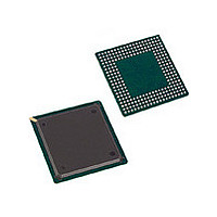
CYP15G0402DXB-BGI Cypress Semiconductor Corp, CYP15G0402DXB-BGI Datasheet - Page 10

CYP15G0402DXB-BGI
Manufacturer Part Number
CYP15G0402DXB-BGI
Description
Manufacturer
Cypress Semiconductor Corp
Datasheet
1.CYP15G0402DXB-BGI.pdf
(29 pages)
Specifications of CYP15G0402DXB-BGI
Lead Free Status / RoHS Status
Not Compliant
Document #: 38-02057 Rev. *G
Pin Descriptions
OUTA±
OUTB±
OUTC±
OUTD±
INA±
INB±
INC±
IND±
OELE
BISTLE
RXLE
BOE[7:0]
Analog I/O and Control
Name
CML Differential
Output
LVPECL Differential
Input
LVTTL Input,
asynchronous,
internal pull-up
LVTTL Input,
asynchronous,
internal pull-up
LVTTL Input,
asynchronous,
internal pull-up
LVTTL Input,
asynchronous,
internal pull-up
I/O Characteristics Signal Description
CYP(V)15G0402DXB Quad HOTLink II™ SERDES (continued)
Differential Serial Data Outputs. These PECL-compatible CML outputs (+3.3V refer-
enced) are capable of driving terminated transmission lines or standard fiber-optic trans-
mitter modules.
Differential Serial Data Inputs. These inputs accept the serial data stream for deseri-
alization. The INx± serial streams are passed to the receiver Clock and Data Recovery
(CDR) circuits to extract the data content when INSELx = HIGH.
Serial Driver Output Enable Latch Enable. When OELE = HIGH, the signals on the
BOE[7:0] inputs directly control the OUTx± differential drivers.
When the BOE[x] input is HIGH, the associated OUTx± differential driver is enabled.
When the BOE[x] input is LOW, the associated OUTx± differential driver is powered
down.
When OELE returns LOW, the last values present on BOE[7:0] are captured in the
internal Output enable Latch.
The specific mapping of BOE[7:0] signals to transmit output enables is listed in Table 2.
If the device is reset (TRSTZ is sampled LOW), the latch is reset to disable all outputs.
Transmit and Receive BIST Latch Enable. Active HIGH. When BISTLE = HIGH, the
signals on the BOE[7:0] inputs directly control the transmit and receive BIST enables.
When the BOE[x] input is LOW, the associated transmit or receive channel is configured
to generate or compare the BIST sequence.
When the BOE[x] input is HIGH, the associated transmit or receive channel is configured
for normal data transmission or reception.
When BISTLE returns LOW the last values present on BOE[7:0] are captured in the
internal BIST Enable Latch.
The specific mapping of BOE[7:0] signals to transmit and receive BIST enables is listed
in Table 2.
When the latch is closed, if the device is reset (TRSTZ is sampled LOW), the latch is
reset to disable BIST on all transmit and receive channels.
Receive Channel Power-Control Latch Enable. When RXLE = HIGH, the signals on
the BOE[7:0] directly control the power enables for the receive PLLs and analog logic.
When the BOE[7:0] input is HIGH, the receive channels PLL’s and analog logic are
active.
When the BOE[7:0] input is LOW, the receive channels are in a power-down mode.
When RXLE returns LOW, the last values present on BOE[7:0] are captured in the
internal RX PLL Enable Latch.
The specific mapping of BOE[7:0] signals to the associated receive channel enables is
listed in Table 2.
When the device is reset (TRSTZ = LOW), the latch is reset to disable all receive
channels.
BIST, Serial Output, and Receive Channel Enables.
These inputs are passed to and through the Output Enable Latch when OELE is HIGH,
and captured in this latch when OELE returns LOW.
These inputs are passed to and through the BIST Enable Latch when BISTLE is HIGH,
and captured in this latch when BISTLE returns LOW.
These inputs are passed to and through the Receive Channel Enable Latch when RXLE
is HIGH, and captured in this latch when RXLE returns LOW.
CYP15G0402DXB
CYV15G0402DXB
Page 10 of 29
[+] Feedback


