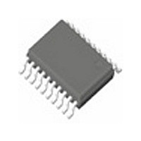
ICS8543BG IDT, Integrated Device Technology Inc, ICS8543BG Datasheet - Page 17

ICS8543BG
Manufacturer Part Number
ICS8543BG
Description
Manufacturer
IDT, Integrated Device Technology Inc
Type
Clock Driverr
Datasheet
1.ICS8543BG.pdf
(18 pages)
Specifications of ICS8543BG
Number Of Clock Inputs
2
Mode Of Operation
Differential
Output Frequency
800MHz
Output Logic Level
LVDS
Operating Supply Voltage (min)
3.135V
Operating Supply Voltage (typ)
3.3V
Operating Supply Voltage (max)
3.465V
Package Type
TSSOP
Operating Temp Range
0C to 70C
Operating Temperature Classification
Commercial
Mounting
Surface Mount
Pin Count
20
Lead Free Status / RoHS Status
Not Compliant
Available stocks
Company
Part Number
Manufacturer
Quantity
Price
Company:
Part Number:
ICS8543BG
Manufacturer:
ICS
Quantity:
365
Company:
Part Number:
ICS8543BG
Manufacturer:
ICSI
Quantity:
12 950
Company:
Part Number:
ICS8543BGILF
Manufacturer:
NUVOTON
Quantity:
5 000
Part Number:
ICS8543BGILFT
Manufacturer:
IDT
Quantity:
20 000
Company:
Part Number:
ICS8543BGLF
Manufacturer:
IDT
Quantity:
755
Part Number:
ICS8543BGLFT
Manufacturer:
IDT
Quantity:
20 000
ICS8543 Data Sheet
Revision History Sheet
ICS8543BG REVISION E DECEMBER 17, 2010
Rev
A
A
A
A
B
C
D
D
D
D
E
E
Table
T4E
T5
4E
T2
T1
T8
T5
T9
6 - 10
Page
10
11
10
13
10
11
12
13
10
11
12
13
16
14
5
3
3
1
5
1
5
2
4
9
2
3
1
6
7
1
Description of Change
In the V
Updated Figure 1, CLK_EN Timing Diagram.
Updated Figure 1, CLK_EN Timing Diagram.
Features section, Bullet 6 to read 3.3V LVDS levels instead of LVPECL.
Updated Parameter Measurement Information figures.
AC Characteristics table - revised Output Frequency from 650MHz to 800MHz.
Features - deleted bullet "Designed to meet or exceed the requirements of
ANSI TIA/EIA-644".
LVDS Table - changed V
Pin Characteristics - changed C
Absolute Maximum Ratings - changed Output rating.
Added Differential Clock Input Interface section.
Added LVPECL Clock Input Interface section.
Added LVDS Driver Termination section.
Updated format throughout data sheet.
Pin Description table - added function description to the OE pin.
Updated LVPECL Clock Input Interface section.
Added Lead Free part number to Ordering Information table.
Updated Figure 1, CLK_EN Timing Diagram.
Updated Differential Clock Input Interface section.
Updated LVPECL Clock Input Interface section.
Added Recommendation for Unused Input and Output Pins section.
Added Power Considerations section.
Updated format throughout the datasheet.
Features section - added Additive Phase Jitter bullet.
AC Characteristics Table - added Added Phase Jitter spec and thermal note.
Added Additive Phase Jitter plot.
Updated Wiring the Differential Input to Accept Single-ended Levels section.
Updated 3.3V Differential Clock Input Interface section.
Updated 3.3V LVPECL Clock Input Interface section.
Updated LVDS Driver Termination section.
Ordering Information Table - deleted “ICS” prefix from Part/Order Number column.
Updated datasheet header/footer style.
Page 1, corrected Header Title.
Power Considerations - corrected typo for junction temperature from 827.7°C to 82.7°C.
OL
row, 1.06 has been moved to the Typical column from the maximum column.
OD
typical value from 350mV to 280mV.
IN
4pF max. to 4pF typical.
17
LOW SKEW, 1-to-4, DIFFERENTIAL-TO-LVDS FANOUT BUFFER
©2010 Integrated Device Technology, Inc.
10/17/01
12/31/03
11/12/10
12/17/10
9/18/01
11/2/01
9/19/02
6/16/04
2/27/08
5/6/02
6/5/02
4/7/04
Date


