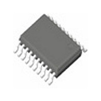
ICS8543BG IDT, Integrated Device Technology Inc, ICS8543BG Datasheet - Page 13

ICS8543BG
Manufacturer Part Number
ICS8543BG
Description
Manufacturer
IDT, Integrated Device Technology Inc
Type
Clock Driverr
Datasheet
1.ICS8543BG.pdf
(18 pages)
Specifications of ICS8543BG
Number Of Clock Inputs
2
Mode Of Operation
Differential
Output Frequency
800MHz
Output Logic Level
LVDS
Operating Supply Voltage (min)
3.135V
Operating Supply Voltage (typ)
3.3V
Operating Supply Voltage (max)
3.465V
Package Type
TSSOP
Operating Temp Range
0C to 70C
Operating Temperature Classification
Commercial
Mounting
Surface Mount
Pin Count
20
Lead Free Status / RoHS Status
Not Compliant
Available stocks
Company
Part Number
Manufacturer
Quantity
Price
Company:
Part Number:
ICS8543BG
Manufacturer:
ICS
Quantity:
365
Company:
Part Number:
ICS8543BG
Manufacturer:
ICSI
Quantity:
12 950
Company:
Part Number:
ICS8543BGILF
Manufacturer:
NUVOTON
Quantity:
5 000
Part Number:
ICS8543BGILFT
Manufacturer:
IDT
Quantity:
20 000
Company:
Part Number:
ICS8543BGLF
Manufacturer:
IDT
Quantity:
755
Part Number:
ICS8543BGLFT
Manufacturer:
IDT
Quantity:
20 000
ICS8543 Data Sheet
Recommendations for Unused Input and Output Pins
Inputs:
CLK/nCLK I
For applications not requiring the use of the differential input, both
CLK and nCLK can be left floating. Though not required, but for
additional protection, a 1kΩ resistor can be tied from CLK to ground.
PCLK/nPCLK I
For applications not requiring the use of the differential input, both
PCLK and nPCLK can be left floating. Though not required, but for
additional protection, a 1kΩ resistor can be tied from PCLK to
ground.
LVCMOS Control Pins
All control pins have internal pull-ups or pull-downs; additional
resistance is not required but can be added for additional protection.
A 1kΩ resistor can be used.
LVDS Driver Termination
A general LVDS interface is shown in Figure 5. Standard termination
for LVDS type output structure requires both a 100Ω parallel resistor
at the receiver and a 100Ω differential transmission line environment.
In order to avoid any transmission line reflection issues, the 100Ω
resistor must be placed as close to the receiver as possible. IDT
offers a full line of LVDS compliant devices with two types of output
structures: current source and voltage source. The standard
Figure 5. Typical LVDS Driver Termination
ICS8543BG REVISION E DECEMBER 17, 2010
LVDS Driver
NPUTS
NPUTS
100Ω Differential Transmission Line
100Ω
13
Outputs:
LVDS Outputs
All unused LVDS outputs should be terminated with 100Ω resistor
between the differential pair.
termination schematic as shown in Figure 5 can be used with either
type of output structure. If using a non-standard termination, it is
recommended to contact IDT and confirm if the output is a current
source or a voltage source type structure. In addition, since these
outputs are LVDS compatible, the amplitude and common mode
input range of the input receivers should be verified for compatibility
with the output.
+
–
LVDS
Receiver
LOW SKEW, 1-to-4, DIFFERENTIAL-TO-LVDS FANOUT BUFFER
©2010 Integrated Device Technology, Inc.


