PDTA115EE,115 NXP Semiconductors, PDTA115EE,115 Datasheet
PDTA115EE,115
Specifications of PDTA115EE,115
934058177115
PDTA115EE T/R


Related parts for PDTA115EE,115


PDTA115EE,115 Summary of contents
Page 1
DATA SHEET PDTA115E series PNP resistor-equipped transistors 100 kΩ 100 kΩ Product data sheet Supersedes data of 2004 May 05 DISCRETE SEMICONDUCTORS 2004 Jul 30 ...
Page 2
... NXP Semiconductors PNP resistor-equipped transistors 100 kΩ 100 kΩ FEATURES • Built-in bias resistors • Simplified circuit design • Reduction of component count • Reduced pick and place costs. APPLICATIONS • General purpose switching and amplification • Inverter and interface circuits • Circuit driver. ...
Page 3
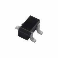
... NXP Semiconductors PNP resistor-equipped transistors 100 kΩ 100 kΩ SIMPLIFIED OUTLINE, SYMBOL AND PINNING TYPE NUMBER PDTA115ES handbook, halfpage PDTA115EE PDTA115EEF handbook, halfpage PDTA115EK PDTA115ET PDTA115EU Top view PDTA115EM handbook, halfpage 2 1 Bottom view 2004 Jul 30 SIMPLIFIED OUTLINE AND SYMBOL MAM338 ...
Page 4
... NXP Semiconductors PNP resistor-equipped transistors 100 kΩ 100 kΩ ORDERING INFORMATION TYPE NUMBER NAME PDTA115EE PDTA115EEF PDTA115EK PDTA115EM PDTA115ES PDTA115ET PDTA115EU LIMITING VALUES In accordance with the Absolute Maximum Rating System (IEC 60134). SYMBOL PARAMETER V collector-base voltage CBO V collector-emitter voltage CEO V emitter-base voltage ...
Page 5
... NXP Semiconductors PNP resistor-equipped transistors 100 kΩ 100 kΩ THERMAL CHARACTERISTICS SYMBOL PARAMETER R thermal resistance from junction to ambient th(j-a) SOT23 SOT54 SOT323 SOT346 SOT416 SOT490 SOT883 Notes 1. Refer to standard mounting conditions. 2. Reflow soldering is the only recommended soldering method. 3. Refer to SOT883 standard mounting conditions; FR4 with 60 μm copper strip line. ...
Page 6
... NXP Semiconductors PNP resistor-equipped transistors 100 kΩ 100 kΩ PACKAGE OUTLINES Plastic surface-mounted package; 3 leads DIMENSIONS (mm are the original dimensions UNIT max 0.30 0.25 0.95 mm 0.1 0.15 0.10 0.60 OUTLINE VERSION IEC SOT416 2004 Jul 0.5 scale 1.8 0.9 1.75 1 0.5 1 ...
Page 7
... NXP Semiconductors PNP resistor-equipped transistors 100 kΩ 100 kΩ Plastic surface-mounted package; 3 leads DIMENSIONS (mm are the original dimensions) UNIT 0.8 0.33 0.2 1.7 mm 0.6 0.23 0.1 1.5 OUTLINE VERSION IEC SOT490 2004 Jul scale 0.95 1.7 0.5 1.0 0.5 0.75 1.5 ...
Page 8
... NXP Semiconductors PNP resistor-equipped transistors 100 kΩ 100 kΩ Plastic surface-mounted package; 3 leads DIMENSIONS (mm are the original dimensions) UNIT 1.3 0.1 0.50 0.26 mm 1.0 0.013 0.35 0.10 OUTLINE VERSION IEC SOT346 2004 Jul scale 3.1 1.7 3.0 1.9 0.95 2.7 1.3 2 ...
Page 9
... NXP Semiconductors PNP resistor-equipped transistors 100 kΩ 100 kΩ Leadless ultra small plastic package; 3 solder lands; body 1.0 x 0 DIMENSIONS (mm are the original dimensions) A (1) 1 UNIT max. 0.50 0.20 0.55 mm 0.03 0.46 0.12 0.47 Note 1. Including plating thickness OUTLINE VERSION ...
Page 10
... NXP Semiconductors PNP resistor-equipped transistors 100 kΩ 100 kΩ Plastic single-ended leaded (through hole) package; 3 leads DIMENSIONS (mm are the original dimensions) UNIT 5.2 0.48 0.66 0.45 mm 5.0 0.40 0.55 0.38 Note 1. Terminal dimensions within this zone are uncontrolled to allow for flow of plastic and terminal irregularities. ...
Page 11
... NXP Semiconductors PNP resistor-equipped transistors 100 kΩ 100 kΩ Plastic surface-mounted package; 3 leads DIMENSIONS (mm are the original dimensions UNIT max. 1.1 0.48 0.15 mm 0.1 0.9 0.38 0.09 OUTLINE VERSION IEC SOT23 2004 Jul scale 3.0 1.4 2.5 1.9 0.95 2.8 1.2 2 ...
Page 12
... NXP Semiconductors PNP resistor-equipped transistors 100 kΩ 100 kΩ Plastic surface-mounted package; 3 leads DIMENSIONS (mm are the original dimensions UNIT b p max 1.1 0.4 0.25 mm 0.1 0.8 0.3 0.10 OUTLINE VERSION IEC SOT323 2004 Jul scale 2.2 1.35 2.2 1.3 0.65 1.8 1 ...
Page 13
... NXP Semiconductors. In case of any inconsistency or conflict between information in this document and such terms and conditions, the latter will prevail. ...
Page 14
... NXP Semiconductors Customer notification This data sheet was changed to reflect the new company name NXP Semiconductors, including new legal definitions and disclaimers. No changes were made to the technical content, except for package outline drawings which were updated to the latest version. Contact information For additional information please visit: http://www ...