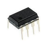
ATTINY12L-4PU Atmel, ATTINY12L-4PU Datasheet - Page 33

ATTINY12L-4PU
Manufacturer Part Number
ATTINY12L-4PU
Description
MCU 8-Bit ATtiny AVR RISC 1KB Flash 3.3V/5V 8-Pin PDIP
Manufacturer
Atmel
Datasheet
1.ATTINY12V-1SI.pdf
(94 pages)
Specifications of ATTINY12L-4PU
Package
8PDIP
Device Core
AVR
Family Name
ATtiny
Maximum Speed
4 MHz
Operating Supply Voltage
3.3|5 V
Data Bus Width
8 Bit
Number Of Programmable I/os
6
Interface Type
SPI
Number Of Timers
1
Program Memory Size
1 KB
Program Memory Type
Flash
Operating Temperature
-40 to 85 °C
Processor Series
ATTINY1x
Core
AVR8
Maximum Clock Frequency
4 MHz
Maximum Operating Temperature
+ 85 C
Mounting Style
Through Hole
Package / Case
PDIP-8
3rd Party Development Tools
EWAVR, EWAVR-BL
Development Tools By Supplier
ATAVRDRAGON, ATSTK500
Minimum Operating Temperature
- 40 C
Lead Free Status / Rohs Status
Details
General Interrupt Mask
Register – GIMSK
1006F–AVR–06/07
• Bits 1, 0 - ISC01, ISC00: Interrupt Sense Control0 Bit 1 and Bit 0
The External Interrupt 0 is activated by the external pin INT0 if the SREG I-flag and the
corresponding interrupt mask are set. The following table shows how to set the ISC bits
to generate an external interrupt:
Table 15. Interrupt 0 Sense Control
The value on the INT0 pin is sampled before detecting edges. If edge interrupt is
selected, pulses that last longer than one CPU clock period will generate an interrupt.
Shorter pulses are not guaranteed to generate an interrupt. If low-level interrupt is
selected, the low level must be held until the completion of the currently executing
instruction to generate an interrupt. If enabled, a level-triggered interrupt will generate
an interrupt request as long as the pin is held low.
• Bit 7 - Res: Reserved Bit
This bit is a reserved bit in the ATtiny11/12 and always reads as zero.
• Bit 6 - INT0: External Interrupt Request 0 Enable
When the INT0 bit is set (one) and the I-bit in the Status Register (SREG) is set (one),
the external pin interrupt is enabled. The Interrupt Sense Control0 bits 1/0 (ISC01 and
ISC00) in the MCU general Control Register (MCUCR) define whether the external
interrupt is activated on rising or falling edge, on pin change, or low level of the INT0 pin.
Activity on the pin will cause an interrupt request even if INT0 is configured as an output.
The corresponding interrupt of External Interrupt Request 0 is executed from program
memory address $001. See also “External Interrupts.”
• Bit 5 - PCIE: Pin Change Interrupt Enable
When the PCIE bit is set (one) and the I-bit in the Status Register (SREG) is set (one),
the interrupt on pin change is enabled. Any change on any input or I/O pin will cause an
interrupt. The corresponding interrupt of Pin Change Interrupt Request is executed from
program memory address $002. See also “Pin Change Interrupt.”
• Bits 4..0 - Res: Reserved Bits
These bits are reserved bits in the ATtiny11/12 and always read as zero.
Bit
$3B
Read/Write
Initial Value
ISC01
0
0
1
1
ISC00
0
1
0
1
R
7
0
-
INT0
R/W
Description
The low level of INT0 generates an interrupt request.
Any change on INT0 generates an interrupt request
The falling edge of INT0 generates an interrupt request.
The rising edge of INT0 generates an interrupt request.
6
0
PCIE
R/W
5
0
R
4
0
-
R
3
0
-
R
2
0
-
ATtiny11/12
R
1
0
-
R
0
0
-
GIMSK
33


