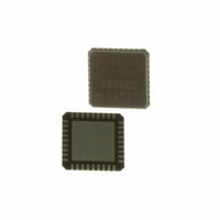
SI5326C-C-GM Silicon Laboratories Inc, SI5326C-C-GM Datasheet - Page 59

SI5326C-C-GM
Manufacturer Part Number
SI5326C-C-GM
Description
DSPLL 36-Pin QFN EP
Manufacturer
Silicon Laboratories Inc
Type
Jitter Attenuatorr
Datasheet
1.SI5326B-C-GM.pdf
(72 pages)
Specifications of SI5326C-C-GM
Package
36QFN EP
Operating Temperature
-40 to 85 °C
Pll
Yes
Input
Clock
Output
CML, CMOS, LVDS, LVPECL
Number Of Circuits
1
Ratio - Input:output
2:2
Differential - Input:output
Yes/Yes
Frequency - Max
346MHz
Divider/multiplier
Yes/Yes
Voltage - Supply
1.71 V ~ 3.63 V
Mounting Type
Surface Mount
Package / Case
36-QFN
Frequency-max
346MHz
Operating Temperature (max)
85C
Operating Temperature (min)
-40C
Package Type
QFN EP
Mounting
Surface Mount
Lead Free Status / RoHS Status
Lead free / RoHS Compliant
Lead Free Status / RoHS Status
Lead free / RoHS Compliant
Other names
336-1746
336-1746-5
336-1746
336-1746-5
336-1746
Available stocks
Company
Part Number
Manufacturer
Quantity
Price
Part Number:
SI5326C-C-GM
Manufacturer:
SILICON LABS/芯科
Quantity:
20 000
Note: Internal register names are indicated by underlined italics, e.g., INT_PIN. See Section “5.Register Map”.
5, 10, 32
Pin #
8, 31
11
15
16
17
12
13
4
7
6
Pin Name
CKIN1+
CKIN1–
CKIN2+
CKIN2–
RATE0
RATE1
GND
C2B
V
XB
XA
DD
GND
V
I/O
O
DD
I
I
I
I
Signal Level
LVCMOS
3-Level
Supply
Analog
Supply
Multi
Multi
CKIN2 Invalid Indicator.
This pin functions as a LOS (and optionally FOS) alarm indicator for
CKIN2 if CK2_BAD_PIN = 1.
0 = CKIN2 present
1 = LOS (FOS) on CKIN2
The active polarity can be changed by CK_BAD_POL. If
CK2_BAD_PIN = 0, the pin tristates.
Supply.
The device operates from a 1.8, 2.5, or 3.3 V supply. Bypass capac-
itors should be associated with the following V
5
10
32
A 1.0 µF should also be placed as close to the device as is practical.
External Crystal or Reference Clock.
External crystal should be connected to these pins to use internal
oscillator based reference. Refer to the Si53xx Family Reference
Manual for interfacing to an external reference. External reference
must be from a high-quality clock source (TCXO, OCXO). Fre-
quency of crystal or external clock is set by RATE[1:0] pins.
Ground.
Must be connected to system ground. Minimize the ground path
impedance for optimal performance of this device. Grounding these
pins does not eliminate the requirement to ground the GND PAD on
the bottom of the package.
External Crystal or Reference Clock Rate.
Three level inputs that select the type and rate of external crystal or
reference clock to be applied to the XA/XB port. Refer to the Si53xx
Family Reference Manual for settings. These pins have both a weak
pull-up and a weak pull-down; they default to M.
L setting corresponds to ground.
M setting corresponds to V
H setting corresponds to V
Note: Tying the corresponding Rate
Some designs may require an external resistor voltage divider when
driven by an active device that will tristate.
Clock Input 1.
Differential input clock. This input can also be driven with a single-
ended signal. Input frequency range is 2 kHz to 710 MHz.
Clock Input 2.
Differential input clock. This input can also be driven with a single-
ended signal. Input frequency range is 2 kHz to 710 MHz.
compatibility to Si5325. Refer to Si5325 data sheet for
operating in this mode.
Rev. 1.0
0.1 µF
0.1 µF
0.1 µF
DD
DD
Description
.
/2.
n
pins to HH (V
DD
pins:
DD
Si5326
) provides
59


