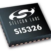
SI5326C-B-GM Silicon Laboratories Inc, SI5326C-B-GM Datasheet

SI5326C-B-GM
Specifications of SI5326C-B-GM
Related parts for SI5326C-B-GM
SI5326C-B-GM Summary of contents
Page 1
Description The Si5326 is a jitter-attenuating precision clock multiplier for applications requiring sub 1 ps jitter performance. The Si5326 accepts dual clock inputs ...
Page 2
Si5326 Table 1. Performance Specifications (V = 1.8, 2.5, or 3.3 V ±10 – º Parameter Symbol Temperature Range T A Supply Voltage V DD Supply Current I DD Input Clock Frequency CK F ...
Page 3
Table 1. Performance Specifications (Continued 1.8, 2.5, or 3.3 V ±10 – º Parameter Symbol Duty Cycle CKO DC PLL Performance Jitter Generation J GEN Jitter Transfer J PK External Reference Jitter ...
Page 4
Si5326 0 -20 -40 -60 -80 -100 -120 -140 -160 100 1000 4 155.52 MHz in, 622.08 MHz out 10000 100000 1000000 Offset Frequency (Hz) Typical Phase Noise Plot Figure 1. Confidential Rev. 0.2 10000000 100000000 ...
Page 5
Figure 2. Si5326 Typical Application Circuit (I Figure 3. Si5326 Typical Application Circuit (SPI Control Mode) Confidential Rev. 0.2 Si5326 2 C Control Mode) 5 ...
Page 6
Si5326 1. Functional Description The Si5326 is a jitter-attenuating precision clock multiplier for applications requiring sub 1 ps jitter performance. The Si5326 accepts dual clock inputs ranging from 2 kHz to 710 MHz and generates two independent, synchronous clock outputs ...
Page 7
Pin Descriptions: Si5326 INT_C1B Pin numbers are preliminary and subject to change. Pin # Pin Name I/O Signal Level 1 I LVCMOS RST 2, 9, 14, NC — 30 INT_C1B O LVCMOS Note: Internal register names are ...
Page 8
Si5326 Pin # Pin Name I/O Signal Level 4 C2B O LVCMOS 5, 10 GND GND 11 RATE0 I 3-Level 15 RATE1 16 CKIN1 CKIN1– 12 ...
Page 9
Pin # Pin Name I/O Signal Level 19 DEC I LVCMOS 20 INC I LVCMOS 21 CS_CA I/O LVCMOS 22 SCL I LVCMOS Note: Internal register names are indicated by underlined italics, e.g. INT_PIN. See Si5326 Register Map. Description Latency ...
Page 10
Si5326 Pin # Pin Name I/O Signal Level 23 SDA_SDO I/O LVCMOS LVCMOS A2_SS I LVCMOS 27 SDI I LVCMOS 29 CKOUT1– CKOUT1+ 34 CKOUT2– CKOUT2+ 36 CMODE I LVCMOS ...
Page 11
... Ordering Guide Ordering Part Output Clock Frequency Number Si5326A-B-GM 2 kHz–945 MHz 970–1134 MHz 1.213–1.417 GHz Si5326B-B-GM 2 kHz–808 MHz Si5326C-B-GM 2 kHz–346 MHz Package Range 36-Lead QFN 36-Lead QFN 36-Lead QFN Confidential Rev. 0.2 Si5326 Temperature Range – °C – ...
Page 12
Si5326 4. Package Outline: 36-Pin QFN Figure 4 illustrates the package details for the Si5326. Table 3 lists the values for the dimensions shown in the illustration. Figure 4. 36-Pin Quad Flat No-lead (QFN) Symbol Millimeters Min Nom A 0.80 ...
Page 13
Recommended PCB Layout Figure 5. PCB Land Pattern Diagram Confidential Rev. 0.2 Si5326 13 ...
Page 14
Si5326 Table 4. PCB Land Pattern Dimensions Dimension Notes (General): 1. All dimensions shown are in millimeters (mm) unless otherwise noted. 2. Dimensioning and Tolerancing is per the ANSI ...
Page 15
OCUMENT HANGE IST Revision 0.1 to Revision 0.2 Updated LVTTL to LVCMOS is Table 2, “Absolute Maximum Ratings,” on page 3. Added Figure 1, “Typical Phase Noise Plot,” on page 4. Updated Figure 2, “Si5326 Typical Application ...
Page 16
... Should Buyer purchase or use Silicon Laboratories products for any such unintended or unauthorized ap- plication, Buyer shall indemnify and hold Silicon Laboratories harmless against all claims and damages. Silicon Laboratories, Silicon Labs, and DSPLL are trademarks of Silicon Laboratories Inc. Other products or brandnames mentioned herein are trademarks or registered trademarks of their respective holders. ...


