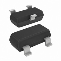
BFR93AR,215 NXP Semiconductors, BFR93AR,215 Datasheet - Page 3

BFR93AR,215
Manufacturer Part Number
BFR93AR,215
Description
TRANS NPN 35MA 12V 6GHZ SOT23
Manufacturer
NXP Semiconductors
Datasheet
1.BFR93AR215.pdf
(13 pages)
Specifications of BFR93AR,215
Package / Case
SOT-23-3, TO-236-3, Micro3™, SSD3, SST3
Transistor Type
NPN
Voltage - Collector Emitter Breakdown (max)
12V
Frequency - Transition
6GHz
Noise Figure (db Typ @ F)
1.9dB ~ 3dB @ 1GHz ~ 2GHz
Power - Max
300mW
Dc Current Gain (hfe) (min) @ Ic, Vce
40 @ 30mA, 5V
Current - Collector (ic) (max)
35mA
Mounting Type
Surface Mount
Dc Collector/base Gain Hfe Min
40 @ 30 mA @ 5 V
Dc Current Gain Hfe Max
40 @ 30mA @ 5V
Minimum Operating Temperature
- 65 C
Mounting Style
SMD/SMT
Configuration
Single
Transistor Polarity
NPN
Maximum Operating Frequency
6000 MHz (Typ)
Collector- Emitter Voltage Vceo Max
12 V
Emitter- Base Voltage Vebo
2 V
Continuous Collector Current
0.035 A
Power Dissipation
300 mW
Maximum Operating Temperature
+ 175 C
Lead Free Status / RoHS Status
Lead free / RoHS Compliant
Gain
-
Lead Free Status / Rohs Status
Lead free / RoHS Compliant
Other names
933653660215
BFR93AR T/R
BFR93AR T/R
BFR93AR T/R
BFR93AR T/R
NXP Semiconductors
6. Thermal characteristics
Table 6.
[1]
7. Characteristics
Table 7.
[1]
[2]
[3]
[4]
BFR93AR_1
Product data sheet
Symbol
R
Symbol
I
h
C
C
C
f
G
NF
V
IMD2
CBO
T
FE
O
th(j-sp)
c
e
re
UM
T
G
Measured on the same crystal in a SOT37 package (BFR91A).
IMD = 60 dB (DIN 45004B); I
V
V
V
measured at f
I
V
V
measured at f
C
G
sp
p
q
r
p
q
UM
= 30 mA; V
= V
UM
= V
= V
= 200 mV at f
= 200 mV at f
is the temperature at the solder point of the collector pin.
is the maximum unilateral power gain, assuming S
O
O
O
=
Thermal characteristics
Characteristics
at IMD = 60 dB; f
Parameter
thermal resistance from junction to solder point
Parameter
collector-base cut-off current
DC current gain
collector capacitance
emitter capacitance
feedback capacitance
transition frequency
unilateral power gain
noise figure
output voltage
second-order intermodulation
distortion
6 dB at f
6 dB at f
10
log
CE
p
p
= 8 V; R
p
p
------------------------------------------------------- - dB.
f
f
r
q
q
1
q
= 250 MHz;
= 560 MHz;
= 805.25 MHz;
= 810 MHz
= 803.25 MHz;
–
f
r
S
= 793.25 MHz
11
L
= 75 ; T
2
p
S
21
= 795.25 MHz;
1
C
2
–
= 30 mA; V
S
22
amb
2
= 25 C;
CE
= 8 V; R
Conditions
I
I
I
see
I
I
T
I
see
I
see
I
T
Figure 13
see
E
C
E
C
C
C
C
C
Rev. 01 — 30 November 2006
amb
amb
f = 1 GHz
f = 2 GHz
f = 1 GHz
f = 2 GHz
= 0 A; V
= 30 mA; V
= i
= i
= i
= 30 mA; V
= 30 mA; V
= 5 mA; V
Figure 4
Figure 5
Figure 6
Figure 15
e
c
c
= 25 C
= 25 C; see
L
12
= 0 A; V
= 0 A; V
= 0 A; V
= 75 ; T
is zero and
CB
CE
to
= 5 V
CE
CE
CE
CB
EB
CE
Conditions
T
amb
= 8 V;
Figure 9
sp
= 5 V; see
= 5 V; f = 500 MHz;
= 8 V; T
= 0.5 V; f = 1 MHz
= 5 V; f = 1 MHz;
= 5 V; f = 1 MHz;
Figure 12
= 25 C;
95 C
S
amb
=
Figure 3
opt
= 25 C;
and
;
NPN 6 GHz wideband transistor
[2][3]
[2][4]
[1]
Min
-
40
-
-
-
4.5
-
-
-
-
-
-
[1]
Typ
260
Typ
-
90
0.7
1.9
0.6
6
13
7
1.9
3
425
BFR93AR
50
© NXP B.V. 2006. All rights reserved.
Max
50
-
-
-
-
-
-
-
-
-
-
-
Unit
K/W
Unit
nA
pF
pF
pF
GHz
dB
dB
dB
dB
mV
dB
3 of 13


