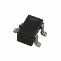
BFS520,115 NXP Semiconductors, BFS520,115 Datasheet - Page 2

BFS520,115
Manufacturer Part Number
BFS520,115
Description
TRANS NPN 70MA 15V 9GHZ SOT323
Manufacturer
NXP Semiconductors
Datasheet
1.BFS520115.pdf
(13 pages)
Specifications of BFS520,115
Package / Case
SC-70-3, SOT-323-3
Transistor Type
NPN
Voltage - Collector Emitter Breakdown (max)
15V
Frequency - Transition
9GHz
Noise Figure (db Typ @ F)
1.1dB ~ 2.1dB @ 900MHz
Power - Max
300mW
Dc Current Gain (hfe) (min) @ Ic, Vce
60 @ 20mA, 6V
Current - Collector (ic) (max)
70mA
Mounting Type
Surface Mount
Dc Current Gain Hfe Max
60 @ 20mA @ 6V
Minimum Operating Temperature
- 65 C
Mounting Style
SMD/SMT
Configuration
Single
Transistor Polarity
NPN
Maximum Operating Frequency
9000 MHz (Typ)
Collector- Emitter Voltage Vceo Max
15 V
Emitter- Base Voltage Vebo
2.5 V
Continuous Collector Current
0.07 A
Power Dissipation
300 mW
Maximum Operating Temperature
+ 175 C
Lead Free Status / RoHS Status
Lead free / RoHS Compliant
Gain
-
Lead Free Status / Rohs Status
Lead free / RoHS Compliant
Other names
568-1654-2
934021420115
BFS520 T/R
934021420115
BFS520 T/R
Available stocks
Company
Part Number
Manufacturer
Quantity
Price
Part Number:
BFS520,115
Manufacturer:
NXP/恩智浦
Quantity:
20 000
NXP Semiconductors
FEATURES
High power gain
Low noise figure
High transition frequency
Gold metallization ensures
SOT323 envelope.
DESCRIPTION
NPN transistor in a plastic SOT323
envelope.
QUICK REFERENCE DATA
LIMITING VALUES
In accordance with the Absolute Maximum System (IEC 134).
Note
1. T
September 1995
V
V
I
P
h
f
G
F
V
V
V
I
P
T
T
SYMBOL
C
T
C
SYMBOL
FE
excellent reliability
stg
j
CBO
CES
tot
CBO
CES
EBO
tot
NPN 9 GHz wideband transistor
UM
s
is the temperature at the soldering point of the collector tab.
collector-base voltage
collector-emitter voltage
DC collector current
total power dissipation
DC current gain
transition frequency
maximum unilateral power gain
noise figure
collector-base voltage
collector-emitter voltage
emitter-base voltage
DC collector current
total power dissipation
storage temperature
junction temperature
PARAMETER
PARAMETER
It is intended for wideband
applications such as satellite TV
tuners, cellular phones, cordless
phones, pagers etc., with signal
frequencies up to 2 GHz.
PINNING
PIN
1
2
3
open emitter
R
up to T
I
I
T
I
T
I
T
C
C
c
c
amb
amb
amb
BE
= 20 mA; V
= 5 mA; V
= 20 mA; V
= 20 mA; V
base
emitter
collector
= 0
open emitter
R
open collector
up to T
= 25 C
= 25 C
= 25 C
BE
s
Code: N2
= 118 C; note 1
DESCRIPTION
= 0
CONDITIONS
2
CE
s
CE
= 118 C; note 1
CE
CE
= 6 V; f = 900 MHz;
= 6 V; f = 900 MHz;
= 6 V; T
= 6 V; f = 1 GHz;
CONDITIONS
j
= 25 C
handbook, 2 columns
60
MIN.
Top view
65
Fig.1 SOT323.
MIN.
120
9
15
1.1
TYP.
Product specification
1
20
15
2.5
70
300
150
175
3
MAX.
20
15
70
300
250
1.6
MAX.
BFS520
MBC870
2
V
V
V
mA
mW
C
C
UNIT
V
V
mA
mW
GHz
dB
dB
UNIT


