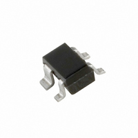
BF1202WR,115 NXP Semiconductors, BF1202WR,115 Datasheet - Page 3

BF1202WR,115
Manufacturer Part Number
BF1202WR,115
Description
MOSFET N-CH DUAL GATE 6V CMPAK-4
Manufacturer
NXP Semiconductors
Datasheet
1.BF1202WR115.pdf
(15 pages)
Specifications of BF1202WR,115
Package / Case
CMPAK-4
Transistor Type
N-Channel Dual Gate
Frequency
400MHz
Gain
30.5dB
Voltage - Rated
10V
Current Rating
30mA
Noise Figure
0.9dB
Current - Test
12mA
Voltage - Test
5V
Configuration
Single Dual Gate
Continuous Drain Current
0.03 A
Drain-source Breakdown Voltage
10 V
Gate-source Breakdown Voltage
6 V
Maximum Operating Temperature
+ 150 C
Minimum Operating Temperature
- 65 C
Mounting Style
SMD/SMT
Power Dissipation
200 mW
Transistor Polarity
N-Channel
Lead Free Status / RoHS Status
Lead free / RoHS Compliant
Power - Output
-
Lead Free Status / Rohs Status
Lead free / RoHS Compliant
Other names
934055958115
BF1202WR T/R
BF1202WR T/R
BF1202WR T/R
BF1202WR T/R
NXP Semiconductors
LIMITING VALUES
In accordance with the Absolute Maximum Rating System (IEC 60134).
Note
1. T
THERMAL CHARACTERISTICS
2010 Sep 16
handbook, halfpage
V
I
I
I
P
T
T
R
SYMBOL
D
G1
G2
SYMBOL
stg
j
DS
tot
N-channel dual-gate PoLo MOS-FETs
th j-s
(1) BF1202WR.
(2) BF1202; BF1202R.
(mW)
s
P tot
250
200
150
100
is the temperature of the soldering point of the source lead.
50
0
0
drain-source voltage
drain current
gate 1 current
gate 2 current
total power dissipation
storage temperature
operating junction temperature
thermal resistance from junction to soldering point
Fig.4 Power derating curve.
BF1202; BF1202R
BF1202WR
BF1202; BF1202R
BF1202WR
50
PARAMETER
100
(2)
(1)
150
T s (°C)
PARAMETER
MCD951
200
T
T
s
s
113 C; note 1
119 C; note 1
3
CONDITIONS
BF1202; BF1202R; BF1202WR
65
MIN.
VALUE
185
155
10
30
10
10
200
200
+150
150
Product specification
MAX.
UNIT
K/W
K/W
V
mA
mA
mA
mW
mW
C
C
UNIT


