BF1202WR,115 NXP Semiconductors, BF1202WR,115 Datasheet - Page 2
BF1202WR,115
Manufacturer Part Number
BF1202WR,115
Description
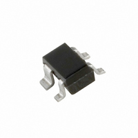
MOSFET N-CH DUAL GATE 6V CMPAK-4
Manufacturer
NXP Semiconductors
Datasheet
1.BF1202WR115.pdf
(15 pages)
Specifications of BF1202WR,115
Package / Case
CMPAK-4
Transistor Type
N-Channel Dual Gate
Frequency
400MHz
Gain
30.5dB
Voltage - Rated
10V
Current Rating
30mA
Noise Figure
0.9dB
Current - Test
12mA
Voltage - Test
5V
Configuration
Single Dual Gate
Continuous Drain Current
0.03 A
Drain-source Breakdown Voltage
10 V
Gate-source Breakdown Voltage
6 V
Maximum Operating Temperature
+ 150 C
Minimum Operating Temperature
- 65 C
Mounting Style
SMD/SMT
Power Dissipation
200 mW
Transistor Polarity
N-Channel
Lead Free Status / RoHS Status
Lead free / RoHS Compliant
Power - Output
-
Lead Free Status / Rohs Status
Lead free / RoHS Compliant
Other names
934055958115
BF1202WR T/R
BF1202WR T/R
BF1202WR T/R
BF1202WR T/R


NXP Semiconductors
FEATURES
Short channel transistor with high
Low noise gain controlled amplifier
Partly internal self-biasing circuit to
APPLICATIONS
VHF and UHF applications with
DESCRIPTION
Enhancement type N-channel
field-effect transistor with source and
substrate interconnected. Integrated
diodes between gates and source
protect against excessive input
voltage surges. The BF1202,
BF1202R and BF1202WR are
encapsulated in the SOT143B,
SOT143R and SOT343R plastic
packages respectively.
QUICK REFERENCE DATA
2010 Sep 16
V
I
P
y
C
C
F
X
T
SYMBOL
This product is supplied in anti-static packing to prevent damage caused by electrostatic discharge during transport
and handling.
D
forward transfer admittance to input
capacitance ratio
ensure good cross-modulation
performance during AGC and good
DC stabilization.
3 to 9 V supply voltage, such as
digital and analogue television
tuners and professional
communications equipment.
j
DS
tot
mod
N-channel dual-gate PoLo MOS-FETs
ig1-ss
rss
fs
drain-source voltage
drain current
total power dissipation
forward transfer admittance
input capacitance at gate 1
reverse transfer capacitance
noise figure
cross-modulation
operating junction temperature
PARAMETER
PINNING
Marking code legend:
handbook, 2 columns
* = - : made in Hong Kong
* = p : made in Hong Kong
* = t : made in Malaysia
BF1202 marking code: LD*
Fig.1
PIN
1
2
3
4
f = 800 MHz
input level for k = 1% at
f = 1 MHz
40 dB AGC
Top view
4
1
Simplified outline
(SOT143B).
CAUTION
CONDITIONS
2
source
drain
gate 2
gate 1
DESCRIPTION
MSB014
3
2
BF1202; BF1202R; BF1202WR
25
100
lfpage
MIN.
handbook, 2 columns
BF1202R marking code: LE*
Fig.2
BF1202WR marking code: LE*
Fig.3
30
1.7
15
1.1
105
TYP.
3
2
Top view
3
2
Top view
Simplified outline
(SOT143R).
Simplified outline
(SOT343R).
Product specification
10
30
200
40
2.2
30
1.8
150
MAX.
MSB842
4
1
MSB035
4
1
V
mA
mW
mS
pF
fF
dB
dBV
C
UNIT
Related parts for BF1202WR,115
Image
Part Number
Description
Manufacturer
Datasheet
Request
R

Part Number:
Description:
Enhancement type Field-Effect Transistor in a plastic SOT343R package
Manufacturer:
NXP Semiconductors
Datasheet:

Part Number:
Description:
MOSFET 2N-CH 10V 30MA SOT343R
Manufacturer:
NXP Semiconductors
Datasheet:

Part Number:
Description:
BOARD-BOARD CONNECTOR SOCKET, 6WAY, 2ROW
Manufacturer:
GLOBAL CONNECTOR TECHNOLOGY
Datasheet:
Part Number:
Description:
BOARD-BOARD CONNECTOR SOCKET, 8WAY, 2ROW
Manufacturer:
GLOBAL CONNECTOR TECHNOLOGY
Datasheet:
Part Number:
Description:
BOARD-BOARD CONN, SOCKET, 10WAY, 2ROW
Manufacturer:
GLOBAL CONNECTOR TECHNOLOGY
Datasheet:

Part Number:
Description:
6w, 2mm Socket, DIL, SMT, Vert, D/Ent, No Peg, GF, Tube
Manufacturer:
GLOBAL CONNECTOR TECHNOLOGY
Part Number:
Description:
8w, 2mm Socket, DIL, SMT, Vert, D/Ent, No Peg, GF, Tube
Manufacturer:
GLOBAL CONNECTOR TECHNOLOGY
Part Number:
Description:
10w, 2mm Socket, DIL, SMT, Vert, D/Ent, No Peg, GF, Tube
Manufacturer:
GLOBAL CONNECTOR TECHNOLOGY
Part Number:
Description:
12w, 2mm Socket, DIL, SMT, Vert, D/Ent, No Peg, GF, Tube
Manufacturer:
GLOBAL CONNECTOR TECHNOLOGY
Part Number:
Description:
14w, 2mm Socket, DIL, SMT, Vert, D/Ent, No Peg, GF, Tube
Manufacturer:
GLOBAL CONNECTOR TECHNOLOGY

Part Number:
Description:
NXP Semiconductors designed the LPC2420/2460 microcontroller around a 16-bit/32-bitARM7TDMI-S CPU core with real-time debug interfaces that include both JTAG andembedded trace
Manufacturer:
NXP Semiconductors
Datasheet:

Part Number:
Description:
NXP Semiconductors designed the LPC2458 microcontroller around a 16-bit/32-bitARM7TDMI-S CPU core with real-time debug interfaces that include both JTAG andembedded trace
Manufacturer:
NXP Semiconductors
Datasheet:
Part Number:
Description:
NXP Semiconductors designed the LPC2468 microcontroller around a 16-bit/32-bitARM7TDMI-S CPU core with real-time debug interfaces that include both JTAG andembedded trace
Manufacturer:
NXP Semiconductors
Datasheet:
Part Number:
Description:
NXP Semiconductors designed the LPC2470 microcontroller, powered by theARM7TDMI-S core, to be a highly integrated microcontroller for a wide range ofapplications that require advanced communications and high quality graphic displays
Manufacturer:
NXP Semiconductors
Datasheet:
Part Number:
Description:
NXP Semiconductors designed the LPC2478 microcontroller, powered by theARM7TDMI-S core, to be a highly integrated microcontroller for a wide range ofapplications that require advanced communications and high quality graphic displays
Manufacturer:
NXP Semiconductors
Datasheet: