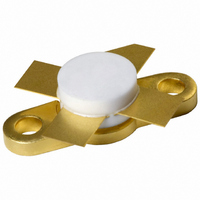
BLF175,112 NXP Semiconductors, BLF175,112 Datasheet - Page 7

BLF175,112
Manufacturer Part Number
BLF175,112
Description
TRANSISTOR RF DMOS SOT123A
Manufacturer
NXP Semiconductors
Datasheet
1.BLF175112.pdf
(21 pages)
Specifications of BLF175,112
Package / Case
SOT-123A
Transistor Type
N-Channel
Frequency
108MHz
Gain
20dB
Voltage - Rated
125V
Current Rating
4A
Current - Test
30mA
Voltage - Test
50V
Power - Output
30W
Minimum Operating Temperature
- 65 C
Mounting Style
SMD/SMT
Resistance Drain-source Rds (on)
1.5 Ohm @ 10 V
Transistor Polarity
N-Channel
Configuration
Single Dual Source
Drain-source Breakdown Voltage
125 V
Gate-source Breakdown Voltage
+/- 20 V
Continuous Drain Current
4 A
Power Dissipation
68000 mW
Maximum Operating Temperature
+ 200 C
Application
HF/VHF
Channel Type
N
Channel Mode
Enhancement
Drain Source Voltage (max)
125V
Output Power (max)
30W
Power Gain (typ)@vds
44@50V/24@50V/20@50VdB
Frequency (max)
108MHz
Package Type
SOT-123A
Pin Count
4
Forward Transconductance (typ)
1.6S
Drain Source Resistance (max)
1500@10Vmohm
Input Capacitance (typ)@vds
130@50VpF
Output Capacitance (typ)@vds
36@50VpF
Reverse Capacitance (typ)
3.7@50VpF
Operating Temp Range
-65C to 200C
Drain Efficiency (typ)
65%
Mounting
Screw
Mode Of Operation
CW Class B/Class-A/Class-AB
Number Of Elements
1
Power Dissipation (max)
68000mW
Vswr (max)
50
Screening Level
Military
Lead Free Status / RoHS Status
Lead free / RoHS Compliant
Noise Figure
-
Lead Free Status / Rohs Status
Lead free / RoHS Compliant
Other names
568-2400
933939780112
BLF175
BLF175
933939780112
BLF175
BLF175
Philips Semiconductors
2003 Jul 22
handbook, halfpage
handbook, halfpage
HF/VHF power MOS transistor
Class-A operation; V
R
solid line: T
dotted line: T
Fig.9
Class-A operation; V
P
Fig.11 Power gain as a function of frequency;
L
GS
(dB)
(dB)
= 8 W (PEP); R
G p
G p
40
30
20
10
= 24 ; f
40
30
20
10
0
0
0
0
Power gain as a function of load power;
typical values.
typical values.
h
= 25 C.
h
1
= 70 C.
= 28.000 MHz; f
GS
10
5
DS
DS
= 24 ; f
= 50 V; I
= 50 V; I
1
2
= 28.001 MHz.
DQ
DQ
10
20
f
2
= 1 MHz.
= 0.8 A;
= 0.8 A;
15
30
P L (W) PEP
f (MHz)
MGP069
MGP071
20
40
7
handbook, halfpage
handbook, halfpage
Class-A operation; V
R
solid line: T
dotted line: T
Fig.10 Third order intermodulation distortion as a
Class-A operation; V
P
Fig.12 Third order intermodulation distortion as a
L
GS
(dB)
(dB)
d 3
= 8 W (PEP); R
d 3
= 24 ; f
20
40
60
80
20
40
60
0
0
0
function of load power; typical values.
function of frequency; typical values.
h
= 25 C.
h
1
= 70 C.
= 28.000 MHz; f
GS
10
DS
DS
5
= 24 ; f
= 50 V; I
= 50 V; I
1
2
= 28.001 MHz.
DQ
DQ
10
20
f
2
= 1 MHz.
= 0.8 A;
= 0.8 A;
Product specification
15
30
P L (W) PEP
f (MHz)
BLF175
MGP070
MGP072
20
40


