IRFR430APBF Vishay, IRFR430APBF Datasheet - Page 4
IRFR430APBF
Manufacturer Part Number
IRFR430APBF
Description
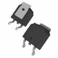
MOSFET N-CH 500V 5A DPAK
Manufacturer
Vishay
Datasheet
1.IRFR430APBF.pdf
(8 pages)
Specifications of IRFR430APBF
Fet Type
MOSFET N-Channel, Metal Oxide
Fet Feature
Standard
Rds On (max) @ Id, Vgs
1.7 Ohm @ 3A, 10V
Drain To Source Voltage (vdss)
500V
Current - Continuous Drain (id) @ 25° C
5A
Vgs(th) (max) @ Id
4.5V @ 250µA
Gate Charge (qg) @ Vgs
24nC @ 10V
Input Capacitance (ciss) @ Vds
490pF @ 25V
Power - Max
110W
Mounting Type
Surface Mount
Package / Case
DPak, TO-252 (2 leads+tab), SC-63
Transistor Polarity
N Channel
Continuous Drain Current Id
5A
Drain Source Voltage Vds
500V
On Resistance Rds(on)
1.7ohm
Rds(on) Test Voltage Vgs
10V
Threshold Voltage Vgs Typ
4.5V
Lead Free Status / RoHS Status
Lead free / RoHS Compliant
Other names
*IRFR430APBF
Available stocks
Company
Part Number
Manufacturer
Quantity
Price

Part Number:
IRFR430APBF
Manufacturer:
VISHAY/威世
Quantity:
20 000


IRFR430A, IRFU430A, SiHFR430A, SiHFU430A
Vishay Siliconix
www.vishay.com
4
Fig. 6 - Typical Gate Charge vs. Gate-to-Source Voltage
10000
Fig. 5 - Typical Capacitance vs. Drain-to-Source Voltage
1000
100
10
1
12
10
7
5
2
0
1
0
I
D
=
5.0A
V DS , Drain-to-Source Voltage (V)
Q , Total Gate Charge (nC)
4
G
V GS = 0V,
C iss = C gs + C gd , C ds
C rss = C gd
C oss = C ds + C gd
10
V
V
V
8
DS
DS
DS
= 400V
= 250V
= 100V
Coss
Ciss
Crss
f = 1 MHZ
12
100
16
SHORTED
1000
20
100
0.1
100
Fig. 7 - Typical Source-Drain Diode Forward Voltage
10
0.1
10
1
1
0.2
10
Tc = 25°C
Tj = 150°C
Single Pulse
T = 150
Fig. 8 - Maximum Safe Operating Area
J
V DS , Drain-toSource Voltage (V)
V
SD
,Source-to-Drain Voltage (V)
0.5
°
C
100
OPERATION IN THIS AREA
LIMITED BY R DS (on)
0.8
S10-1135-Rev. C, 10-May-10
T = 25
J
10msec
100μsec
1msec
Document Number: 91276
1000
°
C
1.1
V
GS
= 0 V
10000
1.4
Related parts for IRFR430APBF
Image
Part Number
Description
Manufacturer
Datasheet
Request
R

Part Number:
Description:
Power MOSFET(Vdss=100V, Rds(on)=0.21ohm, Id=9.4A)
Manufacturer:
IRF [International Rectifier]
Datasheet:
Part Number:
Description:
Advanced Power MOSFET
Manufacturer:
FAIRCHILD [Fairchild Semiconductor]
Datasheet:

Part Number:
Description:
357-036-542-201 CARDEDGE 36POS DL .156 BLK LOPRO
Manufacturer:
Vishay
Datasheet:
Part Number:
Description:
357-036-542-201 CARDEDGE 36POS DL .156 BLK LOPRO
Manufacturer:
Vishay
Datasheet:
Part Number:
Description:
357-036-542-201 CARDEDGE 36POS DL .156 BLK LOPRO
Manufacturer:
Vishay
Datasheet:
Part Number:
Description:
357-036-542-201 CARDEDGE 36POS DL .156 BLK LOPRO
Manufacturer:
Vishay
Datasheet:
Part Number:
Description:
357-036-542-201 CARDEDGE 36POS DL .156 BLK LOPRO
Manufacturer:
Vishay
Datasheet:
Part Number:
Description:
357-036-542-201 CARDEDGE 36POS DL .156 BLK LOPRO
Manufacturer:
Vishay
Datasheet:
Part Number:
Description:
357-036-542-201 CARDEDGE 36POS DL .156 BLK LOPRO
Manufacturer:
Vishay
Datasheet:
Part Number:
Description:
357-036-542-201 CARDEDGE 36POS DL .156 BLK LOPRO
Manufacturer:
Vishay
Datasheet:
Part Number:
Description:
357-036-542-201 CARDEDGE 36POS DL .156 BLK LOPRO
Manufacturer:
Vishay
Datasheet:
Part Number:
Description:
357-036-542-201 CARDEDGE 36POS DL .156 BLK LOPRO
Manufacturer:
Vishay
Datasheet:
Part Number:
Description:
357-036-542-201 CARDEDGE 36POS DL .156 BLK LOPRO
Manufacturer:
Vishay
Datasheet:
Part Number:
Description:
357-036-542-201 CARDEDGE 36POS DL .156 BLK LOPRO
Manufacturer:
Vishay
Datasheet:
Part Number:
Description:
357-036-542-201 CARDEDGE 36POS DL .156 BLK LOPRO
Manufacturer:
Vishay
Datasheet: