STB19NF20 STMicroelectronics, STB19NF20 Datasheet - Page 9
STB19NF20
Manufacturer Part Number
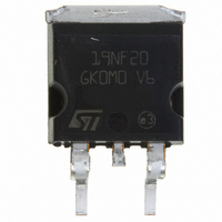
STB19NF20
Description
MOSFET N-CH 200V 15A D2PAK
Manufacturer
STMicroelectronics
Series
MDmesh™r
Datasheet
1.STB19NF20.pdf
(16 pages)
Specifications of STB19NF20
Fet Type
MOSFET N-Channel, Metal Oxide
Fet Feature
Standard
Rds On (max) @ Id, Vgs
160 mOhm @ 7.5A, 10V
Drain To Source Voltage (vdss)
200V
Current - Continuous Drain (id) @ 25° C
15A
Vgs(th) (max) @ Id
4V @ 250µA
Gate Charge (qg) @ Vgs
24nC @ 10V
Input Capacitance (ciss) @ Vds
800pF @ 25V
Power - Max
90W
Mounting Type
Surface Mount
Package / Case
D²Pak, TO-263 (2 leads + tab)
Configuration
Single
Transistor Polarity
N-Channel
Resistance Drain-source Rds (on)
0.16 Ohm @ 10 V
Drain-source Breakdown Voltage
200 V
Gate-source Breakdown Voltage
+/- 20 V
Continuous Drain Current
15 A
Power Dissipation
90000 mW
Maximum Operating Temperature
+ 150 C
Mounting Style
SMD/SMT
Minimum Operating Temperature
- 55 C
Lead Free Status / RoHS Status
Lead free / RoHS Compliant
Other names
497-7941-2
STB19NF20
STB19NF20
Available stocks
Company
Part Number
Manufacturer
Quantity
Price
Company:

Part Number:
STB19NF20
Manufacturer:
ST
Quantity:
12 500


STB19NF20 - STF9NF20 - STP19NF20
3
Figure 15. Switching times test circuit for
Figure 17. Test circuit for inductive load
Figure 19. Unclamped inductive waveform
resistive load
switching and diode recovery times
Test circuit
Figure 16. Gate charge test circuit
Figure 18. Unclamped Inductive load test
Figure 20. Switching time waveform
circuit
Test circuit
9/16
Related parts for STB19NF20
Image
Part Number
Description
Manufacturer
Datasheet
Request
R

Part Number:
Description:
STMicroelectronics [RIPPLE-CARRY BINARY COUNTER/DIVIDERS]
Manufacturer:
STMicroelectronics
Datasheet:
Part Number:
Description:
STMicroelectronics [LIQUID-CRYSTAL DISPLAY DRIVERS]
Manufacturer:
STMicroelectronics
Datasheet:

Part Number:
Description:
BOARD EVAL FOR MEMS SENSORS
Manufacturer:
STMicroelectronics
Datasheet:
Part Number:
Description:
NPN TRANSISTOR POWER MODULE
Manufacturer:
STMicroelectronics
Datasheet:
Part Number:
Description:
TURBOSWITCH ULTRA-FAST HIGH VOLTAGE DIODE
Manufacturer:
STMicroelectronics
Datasheet:
Part Number:
Description:
Manufacturer:
STMicroelectronics
Datasheet:
Part Number:
Description:
DIODE / SCR MODULE
Manufacturer:
STMicroelectronics
Datasheet:
Part Number:
Description:
DIODE / SCR MODULE
Manufacturer:
STMicroelectronics
Datasheet:
Part Number:
Description:
Search -----> STE16N100
Manufacturer:
STMicroelectronics
Datasheet:
Part Number:
Description:
Search ---> STE53NA50
Manufacturer:
STMicroelectronics
Datasheet:
Part Number:
Description:
NPN Transistor Power Module
Manufacturer:
STMicroelectronics
Datasheet:
Part Number:
Description:
DIODE / SCR MODULE
Manufacturer:
STMicroelectronics
Datasheet: