IRLR2905TRPBF International Rectifier, IRLR2905TRPBF Datasheet - Page 2
IRLR2905TRPBF
Manufacturer Part Number
IRLR2905TRPBF
Description
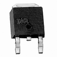
MOSFET N-CH 55V 42A DPAK
Manufacturer
International Rectifier
Series
HEXFET®r
Type
Power MOSFETr
Datasheet
1.IRLR2905TRPBF.pdf
(11 pages)
Specifications of IRLR2905TRPBF
Fet Type
MOSFET N-Channel, Metal Oxide
Fet Feature
Logic Level Gate
Rds On (max) @ Id, Vgs
27 mOhm @ 25A, 10V
Drain To Source Voltage (vdss)
55V
Current - Continuous Drain (id) @ 25° C
42A
Vgs(th) (max) @ Id
2V @ 250µA
Gate Charge (qg) @ Vgs
48nC @ 5V
Input Capacitance (ciss) @ Vds
1700pF @ 25V
Power - Max
110W
Mounting Type
Surface Mount
Package / Case
DPak, TO-252 (2 leads+tab), SC-63
Number Of Elements
1
Polarity
N
Channel Mode
Enhancement
Drain-source On-res
0.027Ohm
Drain-source On-volt
55V
Gate-source Voltage (max)
±16V
Drain Current (max)
42A
Power Dissipation
110W
Output Power (max)
Not RequiredW
Frequency (max)
Not RequiredMHz
Noise Figure
Not RequireddB
Power Gain
Not RequireddB
Drain Efficiency
Not Required%
Operating Temp Range
-55C to 175C
Operating Temperature Classification
Military
Mounting
Surface Mount
Pin Count
2 +Tab
Package Type
DPAK
Lead Free Status / RoHS Status
Lead free / RoHS Compliant
Other names
IRLR2905PBFTR
Available stocks
Company
Part Number
Manufacturer
Quantity
Price
Company:

Part Number:
IRLR2905TRPBF
Manufacturer:
International Rectifier
Quantity:
46 765
Part Number:
IRLR2905TRPBF
Manufacturer:
IR
Quantity:
20 000


‚
ƒ
„
Electrical Characteristics @ T
Source-Drain Ratings and Characteristics
Notes:
L
I
I
V
t
Q
t
V
∆V
R
V
g
I
I
Q
Q
Q
t
t
t
t
L
C
C
C
DSS
SM
rr
on
GSS
d(on)
r
d(off)
f
S
D
fs
S
(BR)DSS
DS(on)
GS(th)
SD
max. junction temperature. ( See fig. 11 )
iss
oss
rss
rr
Repetitive rating; pulse width limited by
V
R
T
Pulse width ≤ 300µs; duty cycle ≤ 2%.
g
gs
gd
I
2
(BR)DSS
SD
J
DD
G
≤ 175°C
= 25Ω, I
≤ 25A, di/dt ≤ 270A/µs, V
= 25V, starting T
/∆T
J
AS
Internal Drain Inductance
Static Drain-to-Source On-Resistance
Drain-to-Source Leakage Current
Continuous Source Current
(Body Diode)
Pulsed Source Current
(Body Diode)
Diode Forward Voltage
Reverse Recovery Time
Reverse RecoveryCharge
Forward Turn-On Time
Drain-to-Source Breakdown Voltage
Breakdown Voltage Temp. Coefficient
Gate Threshold Voltage
Forward Transconductance
Gate-to-Source Forward Leakage
Gate-to-Source Reverse Leakage
Total Gate Charge
Gate-to-Source Charge
Gate-to-Drain ("Miller") Charge
Turn-On Delay Time
Rise Time
Turn-Off Delay Time
Fall Time
Internal Source Inductance
Input Capacitance
Output Capacitance
Reverse Transfer Capacitance
= 25A. (See Figure 12)
J
= 25°C, L =470µH
Parameter
Parameter
DD
≤ V
(BR)DSS
,
J
= 25°C (unless otherwise specified)
–––
–––
–––
–––
–––
–––
–––
–––
–––
–––
–––
–––
–––
–––
–––
–––
–––
–––
Min. Typ. Max. Units
Min. Typ. Max. Units
1.0
–––
–––
55
21
–––
–––
–––
–––
Intrinsic turn-on time is negligible (turn-on is dominated by L
…
†
‡
Caculated continuous current based on maximum allowable
Uses IRLZ44N data and test conditions.
This is applied for I-PAK, L
junction temperature;
lead and center of die contact.
0.070 –––
1700 –––
–––
–––
–––
––– 0.027
––– 0.030
––– 0.040
–––
–––
–––
–––
–––
–––
–––
–––
–––
400
150
–––
210
7.5
4.5
11
84
26
15
80
-100
–––
42 …
–––
–––
250
100
–––
–––
–––
–––
–––
–––
120
320
1.3
2.0
8.6
25
48
25
160
V/°C
nC
nC
nH
µA
nA
pF
ns
ns
W
V
V
S
V
ƒ = 1.0MHz, See Fig. 5‡
MOSFET symbol
showing the
integral reverse
p-n junction diode.
T
T
di/dt = 100A/µs „‡
V
Reference to 25°C, I
V
V
V
V
V
V
V
V
V
I
V
V
V
I
R
R
Between lead,
6mm (0.25in.)
from package
and center of die contact†
V
V
D
D
J
J
GS
GS
GS
GS
DS
DS
DS
DS
GS
GS
DS
GS
DD
GS
DS
G
D
= 25A
= 25A
= 25°C, I
Package limitation current = 20A.
= 25°C, I
= 1.1Ω, See Fig. 10 „‡
= 3.4Ω, V
= 0V, I
= 10V, I
= 5.0V, I
= 4.0V, I
= V
= 25V, I
= 55V, V
= 44V, V
= 16V
= -16V
= 44V
= 5.0V, See Fig. 6 and 13 „‡
= 28V
= 25V
= 0V
S
of D-PAK is measured between
GS
, I
D
F
S
D
D
D
= 250µA
D
D
GS
Conditions
Conditions
= 25A
GS
GS
= 25A, V
= 250µA
= 25A‡
= 25A „
= 25A „
= 21A „
= 5.0V
= 0V
= 0V, T
D
www.irf.com
GS
= 1mA
J
= 150°C
= 0V „
G
G
S
+L
D
D
S
)
S
D
Related parts for IRLR2905TRPBF
Image
Part Number
Description
Manufacturer
Datasheet
Request
R

Part Number:
Description:
Manufacturer:
International Rectifier Corp.
Datasheet:
Part Number:
Description:
SCHOTTKY RECTIFIER
Manufacturer:
International Rectifier Corp.
Datasheet:
Part Number:
Description:
SCHOTTKY RECTIFIER
Manufacturer:
International Rectifier Corp.
Datasheet:
Part Number:
Description:
SCHOTTKY RECTIFIER
Manufacturer:
International Rectifier Corp.
Datasheet:
Part Number:
Description:
SCHOTTKY RECTIFIER
Manufacturer:
International Rectifier Corp.
Datasheet:
Part Number:
Description:
SCHOTTKY RECTIFIER
Manufacturer:
International Rectifier Corp.
Datasheet:
Part Number:
Description:
SCHOTTKY RECTIFIER
Manufacturer:
International Rectifier Corp.
Datasheet:
Part Number:
Description:
SCHOTTKY RECTIFIER
Manufacturer:
International Rectifier Corp.
Datasheet:
Part Number:
Description:
SCHOTTKY RECTIFIER
Manufacturer:
International Rectifier Corp.
Datasheet:
Part Number:
Description:
SCHOTTKY RECTIFIER
Manufacturer:
International Rectifier Corp.
Datasheet:
Part Number:
Description:
SCHOTTKY RECTIFIER
Manufacturer:
International Rectifier Corp.
Datasheet:
Part Number:
Description:
SCHOTTKY RECTIFIER
Manufacturer:
International Rectifier Corp.
Datasheet:
Part Number:
Description:
SCHOTTKY RECTIFIER
Manufacturer:
International Rectifier Corp.
Datasheet:
Part Number:
Description:
SCHOTTKY RECTIFIER
Manufacturer:
International Rectifier Corp.
Datasheet:
Part Number:
Description:
SCHOTTKY RECTIFIER
Manufacturer:
International Rectifier Corp.
Datasheet: