APT18M100B Microsemi Power Products Group, APT18M100B Datasheet

MOSFET N-CH 1000V 18A TO-247

APT18M100B

Manufacturer Part Number
APT18M100B
Description
MOSFET N-CH 1000V 18A TO-247
Manufacturer
Microsemi Power Products Group
Datasheet

Specifications of APT18M100B

Fet Type
MOSFET N-Channel, Metal Oxide
Fet Feature
Standard
Rds On (max) @ Id, Vgs
700 mOhm @ 9A, 10V
Drain To Source Voltage (vdss)
1000V (1kV)
Current - Continuous Drain (id) @ 25° C
18A
Vgs(th) (max) @ Id
5V @ 1mA
Gate Charge (qg) @ Vgs
150nC @ 10V
Input Capacitance (ciss) @ Vds
4845pF @ 25V
Power - Max
625W
Mounting Type
Through Hole
Package / Case
TO-247
Lead Free Status / RoHS Status
Lead free / RoHS Compliant
Other names
APT18M100BMI
APT18M100BMI

Available stocks

Company
Part Number
Manufacturer
Quantity
Price
Part Number:
APT18M100B
Manufacturer:
ST
Quantity:
20 000
Absolute Maximum Ratings
Thermal and Mechanical Characteristics
Symbol
Symbol
T
Torque
Power MOS 8
A proprietary planar stripe design yields excellent reliability and manufacturability. Low
switching loss is achieved with low input capacitance and ultra low C
tance. The intrinsic gate resistance and capacitance of the poly-silicon gate structure
help control slew rates during switching, resulting in low EMI and reliable paralleling,
even when switching at very high frequency. Reliability in fl yback, boost, forward, and
other circuits is enhanced by the high avalanche energy capability.
FEATURES
J
R
R
V
E
I
,T
W
I
• Fast switching with low EMI/RFI
• Low R
• Ultra low C
• Low gate charge
• Avalanche energy rated
• RoHS compliant
P
T
DM
I
AR
θ CS
θ JC
GS
D
AS
D
STG
L
T
DS(on)
Parameter
Continuous Drain Current @ T
Pulsed Drain Current
Gate-Source Voltage
Single Pulse Avalanche Energy
Avalanche Current, Repetitive or Non-Repetitive
Characteristic
Total Power Dissipation @ T
Junction to Case Thermal Resistance
Case to Sink Thermal Resistance, Flat, Greased Surface
Operating and Storage Junction Temperature Range
Soldering Temperature for 10 Seconds (1.6mm from case)
Package Weight
Mounting Torque ( TO-247 Package), 6-32 or M3 screw
rss
is a high speed, high voltage N-channel switch-mode power MOSFET.
for improved noise immunity
N-Channel MOSFET
1
C
= 25°C
C
C
Microsemi Website - http://www.microsemi.com
2
= 25°C
= 100°C
TYPICAL APPLICATIONS
• PFC and other boost converter
• Buck converter
• Two switch forward (asymmetrical bridge)
• Single switch forward
• Flyback
• Inverters
rss
"Miller" capaci-
Min
-55
APT18M100B
Single die MOSFET
1000V, 18A, 0.70Ω Max
Ratings
APT18M100B
APT18M100S
Typ
0.11
0.22
1070
±30
6.2
18
12
68
9
Max
0.20
625
150
300
1.1
APT18M100S
10
D
3
PAK
G
°C/W
in·lbf
Unit
Unit
N·m
mJ
°C
W
oz
A
V
A
g
D
S

Related parts for APT18M100B

APT18M100B Summary of contents

Page 1

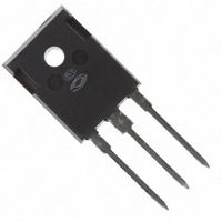
... Two switch forward (asymmetrical bridge) • Single switch forward • Flyback • Inverters = 25° 100° 25°C C Microsemi Website - http://www.microsemi.com APT18M100B APT18M100S 1000V, 18A, 0.70Ω Max 3 D PAK APT18M100B APT18M100S D Single die MOSFET G S Ratings Unit ±30 1070 ...

Page 2

... 25° 100A/µ ≤ 9A, di/dt ≤1000A/µ 125° 4.7Ω 9A. AS with V OSS with V OSS = -1.41E-8 2.48E-9/V + 4.81E-11. o(er APT18M100B_S Min Typ Max I = 250µA 1000 D = 250µA 1. 0.60 0. 1mA D - 25° 125°C J ±100 Min Typ Max ...

Page 3

... DUTY CYCLE GATE-TO-SOURCE VOLTAGE (V) GS Figure 4, Transfer Characteristics 10,000 1,000 100 200 V , DRAIN-TO-SOURCE VOLTAGE (V) DS Figure 6, Capacitance vs Drain-to-Source Voltage 0 SOURCE-TO-DRAIN VOLTAGE (V) SD Figure 8, Reverse Drain Current vs Source-to-Drain Voltage APT18M100B_S = & 4. MAX. DS(ON -55° 25° 125° iss C oss C rss 400 600 ...

Page 4

... Plcs} 0.56 (.022) 0.020 (.001) 2.87 (.113) 0.178 (.007) 3.12 (.123) 2.67 (.105) 1.65 (.065) 2.84 (.112) 2.13 (.084) Gate Drain Source APT18M100B_S I DM 13µs 100µs 1ms 10ms 100ms = 150°C DC line = 25° ...

Related keywords