AD9912/PCBZ Analog Devices Inc, AD9912/PCBZ Datasheet - Page 36
AD9912/PCBZ
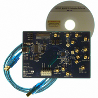
Manufacturer Part Number
AD9912/PCBZ
Description
Eval Board
Manufacturer
Analog Devices Inc
Series
AgileRF™r
Specifications of AD9912/PCBZ
Kit Features
Flexible System Clock I/P Accepts Crystal
Supported Devices
AD9912
Tool / Board Applications
Direct Digital Synthesizer
Development Tool Type
Hardware - Eval/Demo Board
Mcu Supported Families
AD9912
Main Purpose
Timing, Direct Digital Synthesis (DDS)
Embedded
No
Utilized Ic / Part
AD9912
Primary Attributes
14-Bit DAC, 48-Bit Tuning Word Width
Secondary Attributes
1GHz, Graphical User Interface
Lead Free Status / RoHS Status
Lead free / RoHS Compliant
Lead Free Status / RoHS Status
Lead free / RoHS Compliant, Lead free / RoHS Compliant


AD9912
Register 0x01A9—FTW0 (Frequency Tuning Word) (Continued)
Table 27.
Bits
[31:24]
Register 0x01AA—FTW0 (Frequency Tuning Word) (Continued)
Table 28.
Bits
[39:32]
Register 0x01AB—FTW0 (Frequency Tuning Word) (Continued)
Table 29.
Bits
[47:40]
Register 0x01AC—Phase
Table 30.
Bits
[7:0]
Register 0x01AD—Phase (Continued)
Table 31.
Bits
[13:8]
Bit Name
FTW0
Bit Name
FTW0
Bit Name
FTW0
Bit Name
DDS phase word
Bit Name
DDS phase word
Description
These registers contain the FTW (frequency tuning word) for the DDS. The FTW determines the ratio
of the AD9912 output frequency to its DAC system clock. Register 0x01A6 is the least significant
byte of the FTW. Note that the power-up default is defined by start-up Pin S1 to Pin S4. Updates to
the FTW results in an instantaneous frequency jump but no phase discontinuity.
Description
Allows the user to vary the phase of the DDS output. See the Direct Digital Synthesizer section.
Register 0x01AC is the least significant byte of the phase offset word (POW). Note that a momentary
phase discontinuity may occur as the phase passes through 45° intervals.
Description
Allows the user to vary the phase of the DDS output. See the Direct Digital Synthesizer section.
Register 0x01AC is the least significant byte of the phase offset word (POW). Note that a momentary
phase discontinuity may occur as the phase passes through 45° intervals.
Rev. F | Page 36 of 40
Related parts for AD9912/PCBZ
Image
Part Number
Description
Manufacturer
Datasheet
Request
R


Part Number:
Description:
±1.7g Dual-Axis IMEMS Accelerometer Evaluation Board
Manufacturer:
Analog Devices Inc
Datasheet:

Part Number:
Description:
Inertial Sensor Evaluation System
Manufacturer:
Analog Devices Inc
Datasheet:
Part Number:
Description:
Manufacturer:
Analog Devices Inc
Datasheet:
Part Number:
Description:
Manufacturer:
Analog Devices Inc
Datasheet:
Part Number:
Description:
Manufacturer:
Analog Devices Inc
Datasheet:
Part Number:
Description:
Manufacturer:
Analog Devices Inc
Datasheet:
Part Number:
Description:
Manufacturer:
Analog Devices Inc
Datasheet:
Part Number:
Description:
Manufacturer:
Analog Devices Inc
Datasheet:
Part Number:
Description:
Manufacturer:
Analog Devices Inc
Datasheet:
Part Number:
Description:
Manufacturer:
Analog Devices Inc
Datasheet:
Part Number:
Description:
Manufacturer:
Analog Devices Inc
Datasheet:
Part Number:
Description:
Manufacturer:
Analog Devices Inc
Datasheet: