AD9912/PCBZ Analog Devices Inc, AD9912/PCBZ Datasheet
AD9912/PCBZ
Specifications of AD9912/PCBZ


Related parts for AD9912/PCBZ


AD9912/PCBZ Summary of contents
Page 1
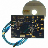
... AD9912 evaluation board. The two versions differ in that Revision B has a convenient connection for a 1 kΩ pull-down resistor on the loop filter pin, whereas Revision A does not. The AD9912/PCBZ operates over an industrial temperature range, spanning −40°C to +85°C. EVALUATION BOARD BLOCK DIAGRAM ...
Page 2
... AD9912/PCBZ TABLE OF CONTENTS Features .............................................................................................. 1 Package Contents .............................................................................. 1 General Description ......................................................................... 1 Evaluation Board Block Diagram ................................................... 1 Revision History ............................................................................... 2 Evaluation Board Physical Connections ....................................... 3 Power Connections ...................................................................... 3 Connections to PC ....................................................................... 3 Signal Connections ...................................................................... 3 Using an Oscillator for the System Clock .................................. 4 Using a Crystal for the System Clock ........................................ 4 Using an External Reconstruction Filter ................................... 4 Evaluation Board Software Setup ................................................... 5 Software Installation ...
Page 3
... CMOS driver (default): connect an oscilloscope/ spectrum analyzer to CMOS_OUT (J7). Note that R106 must be installed to connect J7 to the CMOS out on the AD9912. Connect DUT FILTER OUT (J5) to FDBK IN (J6). Note that this step is not necessary if R20 (near J5) and R18 (near FDBK IN/J6) are stuffed. Rev Page AD9912/PCBZ ...
Page 4
... AD9912/PCBZ • HSTL driver: put a 50 Ω terminator on OUTB (J2), and connect OUT (J1 spectrum analyzer. Connect DUT FILTER OUT (J5) to FDBK IN (J6). Note that this step is not necessary if R20 (near J5) and R18 (near FDBK IN/J6) are stuffed. Enable the HSTL driver in the evaluation software. ...
Page 5
... Interactive Block Diagram window. See the Evaluation Software Main Window section for a description of the main window features, or see the Evaluation Software Functional Blocks section for details on the individual blocks of the AD9912. Rev Page AD9912/PCBZ ...
Page 6
... AD9912/PCBZ EVALUATION SOFTWARE MAIN WINDOW The main window of the evaluation software consists of three major areas: the menu bar, the button bar, and the window display area. The window display area is where windows such as the Interactive Block Diagram window appear. Note that the ...
Page 7
... AD9912 to its default power-up state. I/O Update This button toggles the IO_UPDATE pin on the AD9912. Block Diagram This button selects the Interactive Block Diagram window. Debug Window This button selects the Debug window. See the Debug Window section for a description. Rev Page AD9912/PCBZ ...
Page 8
... AD9912/PCBZ EVALUATION SOFTWARE FUNCTIONAL BLOCKS The AD9912 evaluation software is made up of subsections that correspond to the AD9912’s major functional blocks. These subsections are listed in the following sections, and each of these has its own window. The main window is the Interactive Block Diagram window, and from it, the window for each functional block can be accessed by clicking that block ...
Page 9
... C5 C7 9.70pF 4.70pF 1.50pF 310MHz 370MHz 610MHz 9.0pF 20.0pF 23.0pF PHASE 100M FREQUENCY (Hz) Rev Page AD9912/PCBZ LC combination 8.2 pF combination: C10 = 4.7 pF combination 1.5 pF 14.0pF 50.0Ω EQUIVALENT CIRCUIT FOR TRANSFORMER, IMPEDANCE MATCH, AND AD9912 FDBK_IN 200 MAGNITUDE 150 100 50 0 –50 – ...
Page 10
... AD9912/PCBZ DIFFERENTIAL FILTER DESIGN The differential filter advantages include fewer components and a simpler design when the AD9912 is used in an actual design. Note that the 100 Ω differential source impedance is internal to the IOUT/IOUB driver. Also, note that the ac coupling between the IOUT differential pair and the FDBK_IN differential pair is critical ...
Page 11
... PLL and bipolar edge detector. Table 1. Recommended SYSCLK PLL Loop Filter Values SYSCLK Series R Multiplier (R98) 8 (or less) 390 Ω 10 470 Ω kΩ 40 (default) 2.2 kΩ 60 2.7 kΩ Rev Page AD9912/PCBZ Series C Shunt C (C83) (C88 820 390 180 120 ...
Page 12
... AD9912/PCBZ ORDERING INFORMATION ORDERING GUIDE Model Description 1 AD9912/PCBZ Evaluation Board RoHS Compliant Part ©2008 Analog Devices, Inc. All rights reserved. Trademarks and registered trademarks are the property of their respective owners. EB07190-0-1/08(0) ESD CAUTION Rev Page ...