AD9912/PCBZ Analog Devices Inc, AD9912/PCBZ Datasheet
AD9912/PCBZ
Specifications of AD9912/PCBZ


Related parts for AD9912/PCBZ


AD9912/PCBZ Summary of contents
Page 1
FEATURES 1 GSPS internal clock speed (up to 400 MHz output directly) Integrated 1 GSPS 14-bit DAC 48-bit frequency tuning word with 4 μHz resolution Differential HSTL comparator Flexible system clock input accepts either crystal or external reference clock On-chip ...
Page 2
AD9912 TABLE OF CONTENTS Features .............................................................................................. 1 Applications ....................................................................................... 1 General Description ......................................................................... 1 Basic Block Diagram ........................................................................ 1 Revision History ............................................................................... 3 Specifications ..................................................................................... 4 DC Specifications ......................................................................... 4 AC Specifications .......................................................................... 6 Absolute Maximum Ratings ............................................................ 8 Thermal ...
Page 3
REVISION HISTORY 6/10—Rev Rev. F Changed Default Value of Register 0x003 to 0x19 ( 5/10—Rev Rev. E Deleted 64-Lead LFCSP (CP-64-1) .................................. Universal Changes to SYSCLK PLL Enabled/ Maximum Input Rate of System ............................................................................... 6 Clock ...
Page 4
AD9912 SPECIFICATIONS DC SPECIFICATIONS AVDD = 1.8 V ± 5%, AVDD3 = 3.3 V ± 5%, DVDD = 1.8 V ± 5%, DVDD_I/O = 3.3 V ± 5%, AVSS = 0 V, DVSS = 0 V, unless otherwise noted. Table ...
Page 5
Parameter SYSTEM CLOCK INPUT SYSCLK PLL Bypassed Input Capacitance Input Resistance Internally Generated DC Bias Voltage Differential Input Voltage Swing SYSCLK PLL Enabled Input Capacitance Input Resistance Internally Generated DC Bias Voltage Differential Input Voltage Swing Crystal Resonator with SYSCLK ...
Page 6
AD9912 AC SPECIFICATIONS GHz, DAC kΩ, unless otherwise noted. Power supply pins within the range specified in the DC Specifications section. S SET Table 2. Parameter FDBK_IN INPUT Input Frequency Range Minimum Differential Input ...
Page 7
Parameter CMOS Output Driver (AVDD3/Pin 37) @ 1.8 V Frequency Range Duty Cycle Rise Time/Fall Time (20% to 80%) DAC OUTPUT CHARACTERISTICS st DCO Frequency Range (1 Nyquist Zone) Output Resistance Output Capacitance Full-Scale Output Current Gain Error Output Offset ...
Page 8
AD9912 ABSOLUTE MAXIMUM RATINGS Table 3. Parameter Rating Analog Supply Voltage (AVDD Digital Supply Voltage (DVDD Digital I/O Supply Voltage 3.6 V (DVDD_I/O) DAC Supply Voltage (AVDD3 Pins) 3.6 V Maximum Digital Input Voltage −0.5 V ...
Page 9
PIN CONFIGURATION AND FUNCTION DESCRIPTIONS DVDD_I/O DVSS DVDD DVSS DVDD DVSS DVDD DVSS AVDD AVDD3 NOTES CONNECT. 2. THE EXPOSED PAD MUST BE CONNECTED TO GROUND FOR PROPER OPERATION. Table 5. Pin Function Descriptions Input/ Pin ...
Page 10
AD9912 Input/ Pin No. Output Pin Type 32 I 1.8 V CMOS 33, 39, 43 GND 34 O 1.8 V HSTL 35 O 1.8 V HSTL 37 I Power 38 O 3.3 V CMOS 40 I Differential input ...
Page 11
TYPICAL PERFORMANCE CHARACTERISTICS AVDD, AVDD3, and DVDD at nominal supply voltage; DAC R phase noise used for generating these plots. –50 –55 –60 –65 –70 –75 –80 0 100 200 300 OUTPUT FREQUENCY (MHz) Figure 3. Wideband SFDR vs. Output ...
Page 12
AD9912 10 CARRIER: 0 SFDR: FREQ. SPAN: –10 RESOLUTION BW: VIDEO BW: –20 –30 –40 –50 –60 –70 –80 –90 –100 –110 19.85 19.95 20.05 20.15 FREQUENCY (MHz) Figure 9. Narrow-Band SFDR at 20.1 MHz, SYSCLK = 1 GHz (SYSCLK ...
Page 13
RMS JITTER (100Hz TO 100MHz): 600MHz: 585fs 800MHz: 406fs –110 –120 800MHz –130 600MHz –140 –150 100 1k 10k 100k 1M FREQUENCY OFFSET (Hz) Figure 15. Absolute Phase Noise Using HSTL Driver, SYSCLK = 1 GHz Wenzel Oscillator (SYSCLK ...
Page 14
AD9912 –115 RMS JITTER (100Hz TO 20MHz): 50MHz: 62fs 200MHz: 37fs –125 400MHz: 31fs –135 –145 –155 –165 –175 100 1k 10k 100k FREQUENCY OFFSET (Hz) Figure 21. Absolute Phase Noise of Unfiltered DAC Output MHz, 200 ...
Page 15
NOM SKEW 25°C, 1.8V SUPPLY WORST CASE (SLOW SKEW 90°C, 1.7V SUPPLY) 450 0 200 400 FREQUENCY (MHz) Figure 27. HSTL Output Driver Single-Ended Peak-to-Peak Amplitude vs. Toggle Rate (100 Ω Across Differential Pair) 2.5 2.0 ...
Page 16
AD9912 INPUT/OUTPUT TERMINATION RECOMMENDATIONS 0.01µF AD9912 DOWNSTREAM 1.8V 100Ω HSTL OUTPUT 0.01µF Figure 33. AC-Coupled HSTL Output Driver 50Ω AD9912 DOWNSTREAM 1.8V HSTL AVDD/2 OUTPUT 50Ω Figure 34. DC-Coupled HSTL Output Driver 10pF* AD9912 SELF-BIASING SYSCLK INPUT (CRYSTAL 10pF* MODE) ...
Page 17
THEORY OF OPERATION DIGITAL SYNTHESIS CORE CONFIGURATION LOGIC OVERVIEW The AD9912 is a high performance, low noise, 14-bit DDS clock synthesizer with integrated comparators for applications desiring an agile, finely tuned square or sinusoidal output signal. A ...
Page 18
AD9912 FREQUENCY TUNING WORD (FTW) The input to the DDS is a 48-bit FTW that provides the accu- mulator with a seed value. On each cycle of f adds the value of the FTW to the running total of its ...
Page 19
MAGNITUDE (dB) IMAGE 0 0 –20 PRIMARY –40 –60 –80 SPURS –100 BASE BAND Because the DAC constitutes a sampled system, its output must be filtered so that the analog waveform accurately represents the digital samples supplied to the DAC ...
Page 20
AD9912 SYSCLK INPUTS Functional Description An external time base connects to the AD9912 at the SYSCLK pins to generate the internal high frequency system clock (f The SYSCLK inputs can be operated in one of the following three modes: • ...
Page 21
SYSCLK PLL Multiplier When the SYSCLK PLL multiplier path is employed, the frequency applied to the SYSCLK input pins must be limited so as not to exceed the maximum input frequency of the SYSCLK PLL phase detector. A block diagram ...
Page 22
AD9912 Note that the SYSCLK PLL bypassed and SYSCLK PLL enabled input paths are internally biased level Care should be taken to ensure that any external connections do not disturb the dc bias because ...
Page 23
Although the worst spurs tend to be harmonic in origin, the fact that the DAC is part of a sampled system results in the possibility of spurs appearing in the output spectrum that are not harmoni- cally related to the ...
Page 24
AD9912 THERMAL PERFORMANCE Table 7. Thermal Parameters Symbol Thermal Characteristic Using a JEDEC51-7 Plus JEDEC51-5 2S2P Test Board θ Junction-to-ambient thermal resistance, 0.0 m/sec air flow per JEDEC JESD51-2 (still air) JA θ Junction-to-ambient thermal resistance, 1.0 m/sec air flow ...
Page 25
POWER-UP POWER-ON RESET On initial power-up, the AD9912 internally generates RESET pulse. The pulse is initiated when both of the following two conditions are met: • The 3.3 V supply is greater than 2.35 V ± 0.1 ...
Page 26
AD9912 POWER SUPPLY PARTITIONING The AD9912 features multiple power supplies, and their power consumption varies with its configuration. This section covers which power supplies can be grouped together and how the power consumption of each block varies with frequency. The ...
Page 27
SERIAL CONTROL PORT The AD9912 serial control port is a flexible, synchronous, serial communications port that allows an easy interface with many industry-standard microcontrollers and microprocessors. Single or multiple byte transfers are supported, as well as MSB first or LSB ...
Page 28
AD9912 Read If the instruction word is for a read operation (I15 = 1), the next N × 8 SCLK cycles clock out the data from the address specified in the instruction word, where ...
Page 29
Table 10. Serial Control Port, 16-Bit Instruction Word, MSB First MSB I15 I14 I13 I12 I11 R A12 A11 CSB SCLK DON'T CARE SDIO R A12 A11 A10 DON'T CARE 16-BIT INSTRUCTION HEADER ...
Page 30
AD9912 t S CSB t DS SCLK SDIO BIT N Table 11. Definitions of Terms Used in Serial Control Port Timing Diagrams Parameter Description t Period of SCLK CLK t Read data valid time (time from falling edge of SCLK ...
Page 31
I/O REGISTER MAP All address and bit locations that are left blank in Table 12 are unused. Table 12. Addr 1 (Hex) Type Name Bit 7 Serial port configuration and part identification 0x0000 Serial SDO config. active 0x0001 Reserved 0x0002 ...
Page 32
AD9912 Addr 1 (Hex) Type Name Bit 7 Calibration (user-accessible trim) 0x0400 Reserved to 0x040A 0x040B DAC full- scale 0x040C current 0x040D Reserved 0x040E Reserved 0x040F Reserved and 0x0410 Harmonic spur reduction 0x0500 M Spur A HSR-A enable 0x0501 M ...
Page 33
I/O REGISTER DESCRIPTIONS SERIAL PORT CONFIGURATION (REGISTER 0x0000 TO REGISTER 0x0005) Register 0x0000—Serial Port Configuration Table 13. Bits Bit Name Description [7:4] These bits are the mirror image of Bits[3:0]. 3 Long instruction Read-only; the AD9912 supports only long instructions. ...
Page 34
AD9912 Register 0x0011—Reserved Register 0x0012—Reset (Autoclearing) To reset the entire chip, the user can use the (non-autoclearing) soft reset bit in Register 0x0000. Table 17. Bits Bit Name Description 0 DDS reset Reset of the direct digital synthesis block. Reset ...
Page 35
CMOS OUTPUT DIVIDER (S-DIVIDER) (REGISTER 0x0100 TO REGISTER 0x0106) Register 0x0100 to Register 0x0103—Reserved Register 0x0104—S-Divider Table 21. Bits Bit Name Description [7:0] S-divider CMOS output divider. Divide ratio = 1 − 65,536. If the desired S-divider setting is greater ...
Page 36
AD9912 Register 0x01A9—FTW0 (Frequency Tuning Word) (Continued) Table 27. Bits Bit Name [31:24] FTW0 Register 0x01AA—FTW0 (Frequency Tuning Word) (Continued) Table 28. Bits Bit Name [39:32] FTW0 Register 0x01AB—FTW0 (Frequency Tuning Word) (Continued) Table 29. Bits Bit Name [47:40] FTW0 ...
Page 37
DOUBLER AND OUTPUT DRIVERS (REGISTER 0x0200 TO REGISTER 0x0201) Register 0x0200—HSTL Driver Table 32. Bits Bit Name Description 4 OPOL Output polarity. Setting this bit inverts the HSTL driver output polarity. [3:2] Reserved Reserved. [1:0] HSTL output doubler HSTL output ...
Page 38
AD9912 Register 0x0503—Spur A (Continued) Table 38. Bits Bit Name [7:0] Spur A phase Register 0x0504—Spur A (Continued) Table 39. Bits Bit Name [8] Spur A phase Register 0x0505—Spur B Table 40. Bits Bit Name 7 HSR-B enable 6 Amplitude ...
Page 39
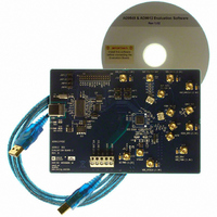
OUTLINE DIMENSIONS PIN 1 INDICATOR TOP VIEW 12° MAX 1.00 0.85 0.80 SEATING PLANE ORDERING GUIDE Model 1 Temperature Range AD9912ABCPZ −40°C to +85°C AD9912ABCPZ-REEL7 −40°C to +85°C AD9912A/PCBZ RoHS Compliant Part. 9.10 9.00 SQ 8.90 0.60 ...
Page 40
AD9912 NOTES ©2007–2010 Analog Devices, Inc. All rights reserved. Trademarks and registered trademarks are the property of their respective owners. D06763-0-6/10(F) Rev Page ...