AD9912/PCBZ Analog Devices Inc, AD9912/PCBZ Datasheet - Page 25
AD9912/PCBZ
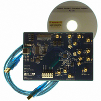
Manufacturer Part Number
AD9912/PCBZ
Description
Eval Board
Manufacturer
Analog Devices Inc
Series
AgileRF™r
Specifications of AD9912/PCBZ
Kit Features
Flexible System Clock I/P Accepts Crystal
Supported Devices
AD9912
Tool / Board Applications
Direct Digital Synthesizer
Development Tool Type
Hardware - Eval/Demo Board
Mcu Supported Families
AD9912
Main Purpose
Timing, Direct Digital Synthesis (DDS)
Embedded
No
Utilized Ic / Part
AD9912
Primary Attributes
14-Bit DAC, 48-Bit Tuning Word Width
Secondary Attributes
1GHz, Graphical User Interface
Lead Free Status / RoHS Status
Lead free / RoHS Compliant
Lead Free Status / RoHS Status
Lead free / RoHS Compliant, Lead free / RoHS Compliant


POWER-UP
POWER-ON RESET
On initial power-up, the AD9912 internally generates a 75 ns
RESET pulse. The pulse is initiated when both of the following
two conditions are met:
•
•
Less than 1 ns after RESET goes high, the S1 to S4 configuration
pins go high impedance and remain high impedance until
RESET is deactivated. This allows strapping and configuration
during RESET.
Because of this reset sequence, external power supply sequenc-
ing is not critical.
DEFAULT OUTPUT FREQUENCY ON POWER-UP
The four status pins (S1 to S4) are used to define the output
frequency of the DDS at power-up even though the I/O registers
have not yet been programmed. At power-up, internal logic
initiates a reset pulse of about 10 ns. During this time, S1 to S4
briefly function as input pins and can be driven externally. Any
logic levels thus applied are transferred to a 4-bit register on the
falling edge of the internally initiated pulse. The same behavior
occurs when the RESET pin is asserted manually.
Setting up S1 to S4 for default DDS startup is accomplished by
connecting a resistor to each pin (either pull-up or pull-down)
to produce the desired bit pattern, yielding 16 possible states
that are used both to address an internal 8 × 16 ROM and to
select the SYSCLK mode (see Table 8). The ROM contains eight
16-bit DDS frequency tuning words (FTWs), one of which is
selected by the state of the S1 to S3 pins. The selected FTW is
transferred to the FTW0 register in the I/O register map
without the need for an I/O update. This ensures that the DDS
generates the selected frequency even if the I/O registers have
not been programmed. The state of the S4 pin selects whether
the internal system clock is generated by means of the internal
SYSCLK PLL multiplier or not (see the SYSCLK Inputs section
for details).
The 3.3 V supply is greater than 2.35 V ± 0.1 V.
The 1.8 V supply is greater than 1.4 V ± 0.05 V.
Rev. F | Page 25 of 40
The DDS output frequency listed in Table 8 assumes that
the internal DAC sampling frequency (f
frequencies scale 1:1 with f
frequencies are available by varying the SYSCLK frequency.
At startup, the internal frequency multiplier defaults to 40×
when the Xtal/PLL mode is selected via the status pins.
Table 8. Default Power-Up Frequency Options for 1 GHz
System Clock
S4
0
0
0
0
0
0
0
0
1
1
1
1
1
1
1
1
Status Pin
S3
0
0
0
0
1
1
1
1
0
0
0
0
1
1
1
1
S2
0
0
1
1
0
0
1
1
0
0
1
1
0
0
1
1
S1
0
1
0
1
0
1
0
1
0
1
0
1
0
1
0
1
SYSCLK
Input Mode
Xtal/PLL
Xtal/PLL
Xtal/PLL
Xtal/PLL
Xtal/PLL
Xtal/PLL
Xtal/PLL
Xtal/PLL
Direct
Direct
Direct
Direct
Direct
Direct
Direct
Direct
S
, meaning that other start-up
S
) is 1 GHz. These
Output Frequency
(MHz)
0
38.87939
51.83411
61.43188
77.75879
92.14783
122.87903
155.51758
0
38.87939
51.83411
61.43188
77.75879
92.14783
122.87903
155.51758
AD9912
Related parts for AD9912/PCBZ
Image
Part Number
Description
Manufacturer
Datasheet
Request
R


Part Number:
Description:
±1.7g Dual-Axis IMEMS Accelerometer Evaluation Board
Manufacturer:
Analog Devices Inc
Datasheet:

Part Number:
Description:
Inertial Sensor Evaluation System
Manufacturer:
Analog Devices Inc
Datasheet:
Part Number:
Description:
Manufacturer:
Analog Devices Inc
Datasheet:
Part Number:
Description:
Manufacturer:
Analog Devices Inc
Datasheet:
Part Number:
Description:
Manufacturer:
Analog Devices Inc
Datasheet:
Part Number:
Description:
Manufacturer:
Analog Devices Inc
Datasheet:
Part Number:
Description:
Manufacturer:
Analog Devices Inc
Datasheet:
Part Number:
Description:
Manufacturer:
Analog Devices Inc
Datasheet:
Part Number:
Description:
Manufacturer:
Analog Devices Inc
Datasheet:
Part Number:
Description:
Manufacturer:
Analog Devices Inc
Datasheet:
Part Number:
Description:
Manufacturer:
Analog Devices Inc
Datasheet:
Part Number:
Description:
Manufacturer:
Analog Devices Inc
Datasheet: