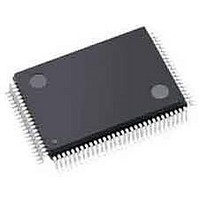
LAN89218AQ SMSC, LAN89218AQ Datasheet - Page 38

LAN89218AQ
Manufacturer Part Number
LAN89218AQ
Description
Ethernet ICs High Perform Chip 10/100 NonPCI Cntrl
Manufacturer
SMSC
Datasheet
1.LAN89218AQ.pdf
(155 pages)
Specifications of LAN89218AQ
Ethernet Connection Type
10BASE-T, 100BASE-TX
Minimum Operating Temperature
- 40 C
Mounting Style
SMD/SMT
Product
Ethernet Controllers
Standard Supported
IEEE802.3, IEEE802.3u
Supply Voltage (max)
3.6 V
Supply Voltage (min)
3 V
Maximum Operating Temperature
+ 85 C
Package / Case
TQFP-100
Lead Free Status / RoHS Status
Lead free / RoHS Compliant
Available stocks
Company
Part Number
Manufacturer
Quantity
Price
Company:
Part Number:
LAN89218AQ
Manufacturer:
RECOM
Quantity:
1 000
Company:
Part Number:
LAN89218AQ
Manufacturer:
SMSC
Quantity:
135
Part Number:
LAN89218AQ-B
Manufacturer:
MICROCHIP/微芯
Quantity:
20 000
Part Number:
LAN89218AQR-B
Manufacturer:
MICROCHIP/微芯
Quantity:
20 000
Revision 1.3 (02-23-10)
3.7.5
Word Swap Function
In addition to mixed endian functionality, the LAN89218 supports a Word Swap Function when its Host
Bus Interface is configured to operate in 16-bit mode. This feature is controlled by the Word Swap
register, which is described in
This register affects how words on the data bus are written to or read from the Control and Status
Registers and the Transmit and Receive Data/Status FIFOs.
Note: The Word Swap register only takes effect when the LAN89218 is configured to operate in 16-
Logic within LAN89218 reorders bytes based on the host bus width (D32/nD16 strap), the setting of
the WORD_SWAP register (16-bit mode of operation only), the state of the endian select signal
(END_SEL), and the state of the least significant address line (A1).
which the word swap and endianess select logic is applied within the LAN89218. Logically, the endian
ordering logic is applied after the word swap logic for write operations, and before the word swap logic
for read operations.
Data path operations for the various supported endianess and word swap configurations are illustrated
in
each type of host access. This figure and table assume an internal byte ordering of 3-2-1-0, where ‘3’
is the most significant byte (data[31:24]) and ‘0’ is the least significant byte (data[7:0]).
CSRs and Status FIFOs
Figure 3.9
bit mode. In 32-bit mode, this register is ignored and the upper data bits, D[31:16], are always
mapped to the high-order word, and the lower data bits, D[15:0], are always mapped to the
low-order word.
and
WORD_SWAP
Figure
END_SEL
3.10. and
Figure 3.8 Host Data Path Diagram
High Performance Single-Chip 10/100 Ethernet Controller for Automotive Applications
Section 5.3.17, "WORD_SWAP—Word Swap Control," on page
Endian Ordering Logic
DATASHEET
(addresses 00h to 3Ch)
(16-bit operation only)
Table 3.9
RX/TX Data FIFO Port
"WORD SWAP"
Host Data Bus
Access
Logic
38
illustrate the byte ordering applied by the endian logic for
RX/TX Data FIFO Direct
Figure 3.8
(FIFO_SEL = 1)
Access
illustrates the order in
SMSC LAN89218
Datasheet
102.


