FW349-TL-E SANYO, FW349-TL-E Datasheet
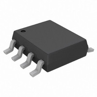
MOSFET N/P-CH 45V 5/4.5A 8-SOP

FW349-TL-E

Manufacturer Part Number
FW349-TL-E
Description
MOSFET N/P-CH 45V 5/4.5A 8-SOP
Manufacturer
SANYO
Datasheet

Specifications of FW349-TL-E

Fet Type
N and P-Channel
Fet Feature
Logic Level Gate
Rds On (max) @ Id, Vgs
37 mOhm @ 5A, 10V
Drain To Source Voltage (vdss)
45V
Current - Continuous Drain (id) @ 25° C
5A, 4.5A
Gate Charge (qg) @ Vgs
18.1nC @ 10V
Input Capacitance (ciss) @ Vds
860pF @ 20V
Power - Max
1.8W
Mounting Type
Surface Mount
Package / Case
8-SOP
Lead Free Status / RoHS Status
Lead free / RoHS Compliant
Vgs(th) (max) @ Id
-
Other names
869-1168-2

Available stocks

Company
Part Number
Manufacturer
Quantity
Price
Part Number:
FW349-TL-E
Manufacturer:
SANYO/三洋
Quantity:
20 000
Ordering number : EN8750
FW349
Features
Specifications
Absolute Maximum Ratings at Ta=25°C
Marking : W349
Drain-to-Source Voltage
Gate-to-Source Voltage
Drain Current (DC)
Drain Current (PW≤10s)
Drain Current (PW≤10µs)
Allowable Power Dissipation
Total Dissipation
Channel Temperature
Storage Temperature
Motor drive application.
Low ON-resistance.
Ultrahigh-speed switching.
Composite type with an N-channel MOSFET and a P-channel MOSFET driving from a 4V supply voltage
contained in a single package.
High-density mounting.
"standard application", intended for the use as general electronics equipment (home appliances, AV equipment,
Any and all SANYO Semiconductor Co.,Ltd. products described or contained herein are, with regard to
communication device, office equipment, industrial equipment etc.). The products mentioned herein shall not be
intended for use for any "special application" (medical equipment whose purpose is to sustain life, aerospace
instrument, nuclear control device, burning appliances, transportation machine, traffic signal system, safety
equipment etc.) that shall require extremely high level of reliability and can directly threaten human lives in case
of failure or malfunction of the product or may cause harm to human bodies, nor shall they grant any guarantee
thereof. If you should intend to use our products for applications outside the standard applications of our
customer who is considering such use and/or outside the scope of our intended standard applications, please
consult with us prior to the intended use. If there is no consultation or inquiry before the intended use, our
customer shall be solely responsible for the use.
Specifications of any and all SANYO Semiconductor Co.,Ltd. products described or contained herein stipulate
the performance, characteristics, and functions of the described products in the independent state, and are not
guarantees of the performance, characteristics, and functions of the described products as mounted in the
customer ' s products or equipment. To verify symptoms and states that cannot be evaluated in an independent
device, the customer should always evaluate and test devices mounted in the customer ' s products or
equipment.
Parameter
TOKYO OFFICE Tokyo Bldg., 1-10, 1 Chome, Ueno, Taito-ku, TOKYO, 110-8534 JAPAN
N-Channel and P-Channel Silicon MOSFETs
General-Purpose Switching Device
Applications
Symbol
V GSS
V DSS
Tstg
I DP
Tch
P T
I D
I D
P D
SANYO Semiconductors
duty cycle≤1%
duty cycle≤1%
Mounted on a ceramic board
(1500mm
Mounted on a ceramic board
(1500mm
FW349
2
2
✕0.8mm)1unit, PW≤10s
✕0.8mm), PW≤10s
Conditions
DATA SHEET
82907PA TI IM TC-00000835
N-channel
--55 to +150
±20
45
20
5
6
150
1.8
2.2
P-channel
--4.5
±20
- -45
- -18
--5
No.8750-1/6
Unit
°C
°C
W
W
V
V
A
A
A

Related parts for FW349-TL-E

FW349-TL-E Summary of contents

Page 1

... To verify symptoms and states that cannot be evaluated in an independent device, the customer should always evaluate and test devices mounted in the customer ' s products or equipment. TOKYO OFFICE Tokyo Bldg., 1-10, 1 Chome, Ueno, Taito-ku, TOKYO, 110-8534 JAPAN FW349 SANYO Semiconductors Symbol Conditions ...

Page 2

... Gate-to-Source Charge Gate-to-Drain “Miller” Charge Diode Forward Voltage Package Dimensions unit : mm (typ) 7005-003 0.43 5.0 1.27 0.595 FW349 Symbol Conditions V (BR)DSS I D =1mA =0V I DSS V DS =45V =0V I GSS V GS =±16V = (off =10V =1mA  yfs  =10V = (on =5A =10V ...

Page 3

... IT12874 [Nch] 100 Ta=25 ° IT12876 [Nch] 10 1.0 0.1 0. 1.0 10 IT12878 --24V --4. =5.33Ω OUT PW=10µs D.C.≤1% G FW349 50Ω =10V 0.5 1.0 1.5 2.0 2.5 Gate-to-Source Voltage (on --60 --40 -- 100 Ambient Temperature ° 0.2 ...

Page 4

... Total Gate Charge --4.5 --4.0 --3.5 --3.0 --2.5 --2.0 --1.5 --1.0 --0 --0.1 --0.2 --0.3 --0.4 --0.5 --0.6 --0.7 Drain-to-Source Voltage (on 160 140 120 --3A 100 --4. --2 --4 --6 --8 --10 Gate-to-Source Voltage FW349 [Nch =24V V GS =10V 2 1000 100 IT12880 [Nch 1 Operation in this area is limited (on). 0 Ta=25° ...

Page 5

... Total Gate Charge 2.6 Mounted on a ceramic board (1500mm 2.4 PW≤10s 2.2 2.0 1.8 1.6 1.4 1.2 1.0 0.8 0.6 0.4 0 100 Ambient Temperature °C FW349 [Pch] -- 10V --1 --0 --0. --10 IT12888 [Pch --24V --10V 3 2 1000 100 7 5 ...

Page 6

... Note on usage : Since the FW349 is a MOSFET product, please avoid using this device in the vicinity of highly charged objects. SANYO Semiconductor Co.,Ltd. assumes no responsibility for equipment failures that result from using products at values that exceed, even momentarily, rated values (such as maximum ratings, operating condition ranges, or other parameters) listed in products specifications of any and all SANYO Semiconductor Co ...

Related keywords