SI3590DV-T1-E3 Vishay, SI3590DV-T1-E3 Datasheet - Page 8
SI3590DV-T1-E3
Manufacturer Part Number
SI3590DV-T1-E3
Description
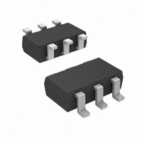
MOSFET N/P-CH 30V 2.5/1.7A 6TSOP
Manufacturer
Vishay
Series
TrenchFET®r
Datasheet
1.SI3590DV-T1-E3.pdf
(9 pages)
Specifications of SI3590DV-T1-E3
Transistor Polarity
N and P-Channel
Fet Type
N and P-Channel
Fet Feature
Logic Level Gate
Rds On (max) @ Id, Vgs
77 mOhm @ 3A, 4.5V
Drain To Source Voltage (vdss)
30V
Current - Continuous Drain (id) @ 25° C
2.5A, 1.7A
Vgs(th) (max) @ Id
1.5V @ 250µA
Gate Charge (qg) @ Vgs
4.5nC @ 4.5V
Power - Max
830mW
Mounting Type
Surface Mount
Package / Case
6-TSOP
Minimum Operating Temperature
- 55 C
Configuration
Dual
Resistance Drain-source Rds (on)
0.077 Ohm @ 4.5 V @ N Channel
Drain-source Breakdown Voltage
30 V
Gate-source Breakdown Voltage
+/- 12 V
Continuous Drain Current
2.5 A @ N Channel or 1.7 A @ P Channel
Power Dissipation
830 mW
Maximum Operating Temperature
+ 150 C
Mounting Style
SMD/SMT
Rds(on) Test Voltage Vgs
12V
Power Dissipation Pd
1.15W
Operating Temperature Range
-55°C To +150°C
No. Of Pins
6
Termination Type
SMD
Lead Free Status / RoHS Status
Lead free / RoHS Compliant
Lead Free Status / RoHS Status
Lead free / RoHS Compliant, Lead free / RoHS Compliant
Other names
SI3590DV-T1-E3TR
Available stocks
Company
Part Number
Manufacturer
Quantity
Price

Part Number:
SI3590DV-T1-E3
Manufacturer:
VISHAY/威世
Quantity:
20 000


Si3590DV
Vishay Siliconix
P-CHANNEL TYPICAL CHARACTERISTICS 25 °C unless noted
Vishay Siliconix maintains worldwide manufacturing capability. Products may be manufactured at one of several qualified locations. Reliability data for Silicon
Technology and Package Reliability represent a composite of all qualified locations. For related documents such as package/tape drawings, part marking, and
reliability data, see www.vishay.com/ppg?72032.
www.vishay.com
8
0.01
0.01
0.1
0.1
2
1
2
1
10
10
-4
-4
Duty Cycle = 0.5
0.2
0.1
0.05
0.02
Duty Cycle = 0.5
0.2
0.1
0.05
0.02
Single Pulse
10
-3
Single Pulse
10
-3
Normalized Thermal Transient Impedance, Junction-to-Ambient
Normalized Thermal Transient Impedance, Junction-to-Foot
10
-2
Square Wave Pulse Duration (s)
Square W ave Pulse Duration (s)
10
-2
10
-1
10
1
-1
1. Duty Cycle, D =
2. Per Unit Base = R
3. T
4. Surface Mounted
1 0
Notes:
P
DM
JM
- T
A
t
1
1
S09-1927-Rev. C, 28-Sep-09
= P
t
2
Document Number: 72032
DM
Z
th J A
th J A
100
t
t
(t )
1
2
= 87 °C/W
600
10
Related parts for SI3590DV-T1-E3
Image
Part Number
Description
Manufacturer
Datasheet
Request
R

Part Number:
Description:
DUAL N/P CH MOSFET, 30V, 2A, TSOP
Manufacturer:
Vishay
Datasheet:

Part Number:
Description:
N- and P-Channel 30-V (D-S) MOSFET
Manufacturer:
Vishay Siliconix
Datasheet:

Part Number:
Description:
357-036-542-201 CARDEDGE 36POS DL .156 BLK LOPRO
Manufacturer:
Vishay
Datasheet:
Part Number:
Description:
357-036-542-201 CARDEDGE 36POS DL .156 BLK LOPRO
Manufacturer:
Vishay
Datasheet:
Part Number:
Description:
357-036-542-201 CARDEDGE 36POS DL .156 BLK LOPRO
Manufacturer:
Vishay
Datasheet:
Part Number:
Description:
357-036-542-201 CARDEDGE 36POS DL .156 BLK LOPRO
Manufacturer:
Vishay
Datasheet:
Part Number:
Description:
357-036-542-201 CARDEDGE 36POS DL .156 BLK LOPRO
Manufacturer:
Vishay
Datasheet:
Part Number:
Description:
357-036-542-201 CARDEDGE 36POS DL .156 BLK LOPRO
Manufacturer:
Vishay
Datasheet:
Part Number:
Description:
357-036-542-201 CARDEDGE 36POS DL .156 BLK LOPRO
Manufacturer:
Vishay
Datasheet:
Part Number:
Description:
357-036-542-201 CARDEDGE 36POS DL .156 BLK LOPRO
Manufacturer:
Vishay
Datasheet:
Part Number:
Description:
357-036-542-201 CARDEDGE 36POS DL .156 BLK LOPRO
Manufacturer:
Vishay
Datasheet:
Part Number:
Description:
357-036-542-201 CARDEDGE 36POS DL .156 BLK LOPRO
Manufacturer:
Vishay
Datasheet:
Part Number:
Description:
357-036-542-201 CARDEDGE 36POS DL .156 BLK LOPRO
Manufacturer:
Vishay
Datasheet:
Part Number:
Description:
357-036-542-201 CARDEDGE 36POS DL .156 BLK LOPRO
Manufacturer:
Vishay
Datasheet:
Part Number:
Description:
357-036-542-201 CARDEDGE 36POS DL .156 BLK LOPRO
Manufacturer:
Vishay
Datasheet: