ZXMC10A816N8TC Diodes Inc, ZXMC10A816N8TC Datasheet - Page 2
ZXMC10A816N8TC
Manufacturer Part Number
ZXMC10A816N8TC
Description
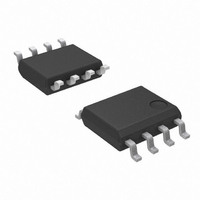
MOSFET DUAL COMPL 100V 8-SOIC
Manufacturer
Diodes Inc
Datasheet
1.ZXMC10A816N8TC.pdf
(11 pages)
Specifications of ZXMC10A816N8TC
Fet Type
N and P-Channel
Fet Feature
Logic Level Gate
Rds On (max) @ Id, Vgs
230 mOhm @ 1A, 10V
Drain To Source Voltage (vdss)
100V
Current - Continuous Drain (id) @ 25° C
2A
Vgs(th) (max) @ Id
3V @ 250µA
Gate Charge (qg) @ Vgs
9.2nC @ 10V
Input Capacitance (ciss) @ Vds
497pF @ 50V
Power - Max
1.8W
Mounting Type
Surface Mount
Package / Case
8-SOIC (3.9mm Width)
Lead Free Status / RoHS Status
Lead free / RoHS Compliant
Other names
ZXMC10A816N8DITR
Available stocks
Company
Part Number
Manufacturer
Quantity
Price
Company:

Part Number:
ZXMC10A816N8TC
Manufacturer:
DIODES
Quantity:
15 000


Absolute maximum ratings
Thermal resistance
NOTES:
(a) For a device surface mounted on 25mm x 25mm x 1.6mm FR4 PCB with high coverage of single sided 1oz copper, in still
(b) Same as note (a), except the device is measured at t
(c)
(d) For a dual device with one active die.
(e) For a device with two active die running at equal power.
(f)
Issue 1.3 - March 2009
© Diodes Incorporated 2009
Parameter
Drain-Source voltage
Gate-Source voltage
Continuous Drain current @ V
Pulsed Drain current @ V
Continuous Source current (Body diode) at T
Pulsed Source current (Body diode) at T
Power dissipation at T
Linear derating factor
Power dissipation at T
Linear derating factor
Power dissipation at T
Linear derating factor
Power dissipation at T
Linear derating factor
Operating and storage temperature range
Parameter
Junction to ambient
Junction to ambient
Junction to ambient
Junction to lead
air conditions; the device is measured when operating in a steady-state condition.
Same as note (a), except the device is pulsed with D= 0.02 and pulse width 300 µs. The pulse current is limited by the
maximum junction temperature.
Thermal resistance from junction to solder-point (at the end of the drain lead); the device is operating in a steady-state
condition.
(f)(d)
(a)(d)
(a)(e)
(b)(d)
A
A
A
L
=25 C
=25 C
=25 C
=25 C
GS
@ V
@ V
@ V
@ V
= 10V; T
GS
GS
GS
GS
GS
(f)(d)
(a)(d)
(a)(e)
(b)(d)
= 10V; T
= 10V; T
= 10V; T
= 10V; T
= 10V; T
A
=25 C
A
A
A
A
A
L
=25 C
=25 C
=70 C
=25 C
=25 C
=25 C
(c)(d)
A
=25 C
(c)(d)
(b)(d)
(b)(d)
(a)(d)
(a)(e)
10 sec.
(f)(d)
2
(b)(d)
Symbol
Symbol
T
V
R
R
R
R
j
V
, T
I
I
P
P
P
P
DSS
I
DM
SM
I
GS
D
S
D
D
D
D
JA
JA
JA
JL
stg
channel
18.9
100
Q1
2.1
1.7
1.7
2.0
2.3
9.4
3.0
9.4
2.4
ZXMC10A816N8
N-
20
53
-55 to 150
Value
10.0
14.2
16.7
100
1.3
1.8
2.1
70
60
www.diodes.com
channel
-10.5
-10.5
-100
20.4
-2.2
-1.8
-1.7
-2.0
-2.4
-3.1
Q2
2.6
P-
20
49
mW/ C
mW/ C
mW/ C
mW/ C
Unit
Unit
C/W
C/W
C/W
C/W
W
W
W
W
V
V
A
A
A
A
C
Related parts for ZXMC10A816N8TC
Image
Part Number
Description
Manufacturer
Datasheet
Request
R

Part Number:
Description:
Diodes (General Purpose, Power, Switching) 240V 350mW
Manufacturer:
Diodes Inc
Datasheet:

Part Number:
Description:
Diodes (General Purpose, Power, Switching) -
Manufacturer:
Diodes Inc
Part Number:
Description:
Diodes (General Purpose, Power, Switching) -
Manufacturer:
Diodes Inc

Part Number:
Description:
Diodes (General Purpose, Power, Switching) NPN Small SIG 50V 45V VCEO 6.0V VEBO
Manufacturer:
Diodes Inc
Datasheet:
Part Number:
Description:
Diodes (General Purpose, Power, Switching) NPN Small SIG 30V 30V VCEO 5.0V VEBO
Manufacturer:
Diodes Inc
Datasheet:
Part Number:
Description:
Diodes (General Purpose, Power, Switching) NPN Small SIG -80V -65V VCEO -5.0 VEBO
Manufacturer:
Diodes Inc
Datasheet:
Part Number:
Description:
Diodes (General Purpose, Power, Switching) NPN Small SIG -50V -45V VCEO 6.0V VEBO
Manufacturer:
Diodes Inc
Part Number:
Description:
Diodes (General Purpose, Power, Switching) Dual Switching DIODE 100V Vrm 75Vrrm 53Vr
Manufacturer:
Diodes Inc
Datasheet:

Part Number:
Description:
Diodes (General Purpose, Power, Switching) Vr/80V Io/125mA T/R
Manufacturer:
Diodes Inc
Datasheet:

Part Number:
Description:
Diodes (General Purpose, Power, Switching) HV DUAL SW DIODE 300V
Manufacturer:
Diodes Inc
Datasheet:

Part Number:
Description:
Diodes (General Purpose, Power, Switching) 80V 150mW
Manufacturer:
Diodes Inc
Datasheet:
Part Number:
Description:
Diodes (General Purpose, Power, Switching) 75V 150mW
Manufacturer:
Diodes Inc
Datasheet:

Part Number:
Description:
Diodes (General Purpose, Power, Switching) 200MW 80V
Manufacturer:
Diodes Inc
Part Number:
Description:
Diodes (General Purpose, Power, Switching) 100V Io/150mA T/R INVALID P/N
Manufacturer:
Diodes Inc

Part Number:
Description:
Diodes (General Purpose, Power, Switching) 350MW 75V
Manufacturer:
Diodes Inc