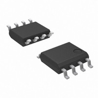
ZXMC10A816N8TC Diodes Inc, ZXMC10A816N8TC Datasheet

ZXMC10A816N8TC
Specifications of ZXMC10A816N8TC
Available stocks
Related parts for ZXMC10A816N8TC
ZXMC10A816N8TC Summary of contents
Page 1
... Fast switching speed Low voltage (V = 4.5 V) gate drive GS Applications DC motor control Backlighting Class D Audio Output Stages (<100W) Ordering information Device Reel size (inches) ZXMC10A816N8TC 13 Device marking ZXMC 10A816 Issue 1.3 - March 2009 © Diodes Incorporated 2009 A Product Line of Diodes Incorporated I (A) D ...
Page 2
... For a dual device with one active die. (e) For a device with two active die running at equal power. (f) Thermal resistance from junction to solder-point (at the end of the drain lead); the device is operating in a steady-state condition. Issue 1.3 - March 2009 © Diodes Incorporated 2009 (b)(d) = 10V (b)(d) = 10V ...
Page 3
... Pulse Width (s) Transient Thermal Impedance 100 10 1 100µ 1m 10m 100m Pulse Width (s) Pulse Power Dissipation Issue 1.3 - March 2009 © Diodes Incorporated 2009 10 R Limited 1 100m 10ms Note (a)(d) 1ms 10m 100us Single Pulse, T 0.1 10 100 P-channel Safe Operating Area 2 ...
Page 4
... Reverse recovery charge NOTES: (a) Measured under pulsed conditions. Pulse width (b) Switching characteristics are independent of operating junction temperature. (c) For design aid only, not subject to production testing Issue 1.3 - March 2009 © Diodes Incorporated 2009 = 25° C unless otherwise stated) amb Min. Typ. 100 ...
Page 5
... V Gate-Source Voltage (V) GS Typical Transfer Characteristics 0.1 0.01 0.1 I Drain Current (A) D On-Resistance v Drain Current Issue 1.3 - March 2009 © Diodes Incorporated 2009 10V 10 5V 4.5V 4V 3. 2.2 2.0 1.8 1.6 1.4 1 25° C 1.0 0.8 ...
Page 6
... Drain - Source Voltage (V) DS Capacitance v Drain-Source Voltage Test circuits Charge Basic gate charge waveform V DS 90% 10 d(on (on) Switching time waveforms Issue 1.3 - March 2009 © Diodes Incorporated 2009 1. 1MHz RSS 100 Charge (nC) Gate-Source Voltage v Gate Charge Gate charge test circuit t t d(off ...
Page 7
... Reverse recovery charge NOTES: (a) Measured under pulsed conditions. Pulse width (b) Switching characteristics are independent of operating junction temperature. (c) For design aid only, not subject to production testing Issue 1.3 - March 2009 © Diodes Incorporated 2009 = 25° C unless otherwise stated) amb Min. Typ. -100 ...
Page 8
... Output Characteristics T = 150° 3.0 3.5 4.0 -V Gate-Source Voltage (V) GS Typical Transfer Characteristics -V 3. 0.1 0 Drain Current (A) D On-Resistance v Drain Current Issue 1.3 - March 2009 © Diodes Incorporated 2009 10V T = 150° 4. 3.5V 0 0.01 10 2.0 1.8 1.6 1 25° C 1.2 1.0 0 10V 0 ...
Page 9
... Drain - Source Voltage (V) DS Capacitance v Drain-Source Voltage Test circuits Charge Basic gate charge waveform d(off) t (on) Switching time waveforms Issue 1.3 - March 2009 © Diodes Incorporated 2009 1MHz OSS 4 C RSS 100 0 Gate-Source Voltage v Gate Charge V DS 90% 10 ...
Page 10
... D 0.189 0.197 H 0.228 0.244 E 0.150 0.157 L 0.016 0.050 Note: Controlling dimensions are in inches. Approximate dimensions are provided in millimeters Issue 1.3 - March 2009 © Diodes Incorporated 2009 Millimeters DIM Min. Max. 1.35 1.75 e 0.10 0.25 b 4.80 5.00 c 5.80 6.20 θ ...
Page 11
... Any Customer or user of this document or products described herein in such applications shall assume all risks of such use and will agree to hold Diodes Incorporated and all the companies whose products are represented on Diodes Incorporated website, harmless against all damages. ...


