VS6502V015/T2 STMicroelectronics, VS6502V015/T2 Datasheet
VS6502V015/T2
Specifications of VS6502V015/T2
Available stocks


Related parts for VS6502V015/T2


VS6502V015/T2 Summary of contents
Page 1
... PCB either via a socket or flex option. The socket allows the PCB to use standard reflow soldering techniques. The sensor outputs 10-bit raw digital image data which directly interface to a range of STMicroelectronics companion processors via 4/5 wire interface interface allows the processor to configure the device and control exposure and gain settings ...
Page 2
Table of Contents Chapter 1 Overview . . . . . . . . . . . . . . . . . . . . . . . . . . . . . . . . . . ...
Page 3
VS6502 6.1 Optical characterisation results .......................................................................................... 35 6.2 Blooming ............................................................................................................................ 35 Chapter 7 Defect Categorisation . . . . . . . . . . . . . . . . . . . . . . . . . ...
Page 4
Overview 1 Overview 1.1 Sensor overview The VS6502 image sensor produces raw digital video data frames per second VGA or 60 frames per second QVGA. The image data is digitized using an internal 10-bit ADC. The ...
Page 5
VS6502 1.2 Typical applications USB camera with STV0674 or STV0676 This is a USB video camera where the co-processor supplies the sensor clock CLKIN and uses the embedded control sequences to synchronize with the frame and line level timings. Figure ...
Page 6
Overview 1.3 Module Pad Description 1.3.1 Pad assignment Pad 14 Pad 1 Pad Number Pad Name AVDD 3 AGND DGND 9 SCL 10 SDA 11 DVDD 12 CLKIN ...
Page 7
VS6502 2 Functional Description 2.1 Video block 2.1.1 Overview The analogue core of the video block contains a VGA sized pixel array. The integration time and access for a row of pixels is controlled by the Y-address block. The row ...
Page 8
Functional Description 2.1.2 Imaging array The physical pixel array is 656 x 496 pixels. The pixel size is 5.6 µm by 5.6 µm. The image size is 644 x 484 pixels in VGA and 324 x 244 pixels in QVGA. ...
Page 9
VS6502 2.2 Image Formats 2.2.1 VGA Format This is the default format and produces an output of 644 pixels by 484 pixels. 2.2.2 Sub-sampled QVGA format In this mode the QVGA image is generated by sub-sampling the VGA image in ...
Page 10
Functional Description 2.3 Data format The video interface consists of a mono-directional, tri-stateable 5 wire data bus. There are two data output modes controlled by serial register [23] 4- wire mode: data is 8 bits per pixel, output as two ...
Page 11
VS6502 Frame-level position of QCLK signal QCLK can operate in 2 different modes, selectable using register [20] Free running: in this mode, QCLK is runs continuously Active only: in this mode QCLK only qualifies the visible lines 2.3.2 Line format ...
Page 12
Functional Description 2.3.3 Line Codes All line codes are 8 bit numbers. When the 502 is in 5-wire mode ie outputting 10-bit pixel data then the codes are shifted left by 2 bits i.e. multiplied by 4. Table 2: Line ...
Page 13
... C7 2.3.6.1 Start of Frame (SOF) line timing The start of frame line at the beginning of each video frameframe contains status data. Please contact STMicroelectronics for details. 2.3.6.2 Blank lines The blank lines contain blank bytes (07 2.3.6.3 Dark lines The dark line contains the dark calibrated values of the optically shielded lines. The average value is 16 when dark calibration is enabled ...
Page 14
Functional Description 2.3.7 Image translations The imaging array can be readout with different modes as described here below: Shuffle horizontal readout, bit [7] of serial register [17]. Even columns (2,4,6.) are readout first. Mirror horizontal readout, bit [3] of serial ...
Page 15
VS6502 2.3.9 Clock management and on-chip divider The VS6502 has a built-in clock divider which acts on the input clock as shown in clock divide ratio is controlled by register 37. CLKIN With the user programmable divider set to its ...
Page 16
Functional Description Frame length Line length Exposure Coarse exposure value Fine exposure value Pixel period Exposure time Example of exposure calculation in default VGA video mode coarse exposure = 522 fine exposure = 762 Input clock frequency - Fclkin = ...
Page 17
VS6502 To eliminate the possibility of the sensor array seeing only part of the new exposure and gain settings, if the serial interface communication extends over a frame boundary, the internal re-timing of exposure and gain data is disabled while ...
Page 18
Functional Description 2.5 Mode Control The VS6502 modes are controlled by two I2C registers: Register[16] - Setup0 Register[28] - IDLE mode control On power up, the VS6502 is in low-power mode and bit 0 of register [16] is set. Clearing ...
Page 19
VS6502 3 Serial Control Bus 3.1 General description The 2-wire I2C serial interface bus is used to read and write the sensor control registers. Some status registers are read-only. The main features of the serial interface include: Variable length read/write ...
Page 20
Serial Control Bus 0 The byte following the address byte contains the address of the first data byte (also referred to as the index). The serial interface can address up to 128 byte registers. Sensor acknowledges valid address S address ...
Page 21
VS6502 3.3 Types of messages This section gives guidelines on the basic operations to read data from and write data to the serial interface. The serial interface supports variable length messages. A message may contain no data bytes, one data ...
Page 22
Serial Control Bus condition is asserted between the write and read messages. In this example, the gain value (index = 36 Figure 21: No data write followed by same location read No data write ...
Page 23
VS6502 Register Description 4.1 Register summary The 8-bit registers within the sensor are accessible via the serial interface. Registers are grouped according to their function. The primary register groups for the VS6502 are: Status registers Setup ...
Page 24
I2C Register Description Index Name 37 clk_div 44 dark offsetH 45 dark offsetL 46 dark offset setup Video format registers - [82-98] 82 line_lengthH 83 line_lengthL 87 x-offsetH 88 x-offsetL 90 y-offsetL 97 frame_lengthH 98 frame_lengthL 4.2 Status registers 4.2.1 ...
Page 25
VS6502 4.2.2 [2] - Status0 Bits [7] Video timing parameter update pending flag [4] Odd/even frame [3] Clock division update pending [2] Gain value update pending [1] Coarse exposure value update pending [0] Fine exposure value update pending 4.2.3 [9-10] ...
Page 26
I2C Register Description 4.3 Setup registers 4.3.1 [16] - Setup0 Bits [7:5] Video Timing Mode Select [2] Soft Reset [0] Low-Power setup0 [7:5] 001 100 110 4.3.2 [17] - Shuffle Bits [7] Pixel read-out order [20] - fg_modes 4.3.3 Bits ...
Page 27
VS6502 [22] - shuffle/mirror 4.3.4 Bits [4] Line read-out order (vmirror) [3] Pixel read-out order (hmirror) [23] - op_format 4.3.5 Bits [5] Output tristate control [2] Embedded code control [0] Data format select [28] - Idle Mode Control 4.3.6 Bits ...
Page 28
I2C Register Description 4.4 Exposure Control Registers A set of programmable registers controls the sensitivity of the sensor. The registers are as follows: Fine exposure Coarse exposure time Analogue gain Clock division The gain parameter does not affect the integration ...
Page 29
VS6502 [36] - Analogue gain 4.4.3 Bits [3:0] GAIN [3:0] [37] - Clock Divider 4.4.4 Bits [3:0] Clock divider setting 4.4.5 [44 -45] - Dark Line Pixel Offset Index Bits 44 [2:0] MS Dark line pixel offset 45 [7:0] LS ...
Page 30
I2C Register Description 4.4.6 [46] Dark Line Offset Cancellation Setup Register Table 26: Dark line offset cancellation setup register Bits [0] Apply Dark Offset [1] Offset source 4.5 Video format registers The following registers control the line & frame lengths ...
Page 31
VS6502 5 Electrical Characteristics 5.1 Absolute maximum ratings Symbol V Digital power supply DD V Analogue power supply CC I Digital input current DD T Storage temperature STO T Lead temperature (10 s) JDEC moisture level 3 LEAD a. A ...
Page 32
Electrical Characteristics 5.4 DC electrical characteristics Over operating conditions unless otherwise specified. 5.4.1 Power supply Symbol V Digital power supply range of operation DD V Analogue power supply range of operation CC I Normal mode sensor current consumption VDD±VCC (VGA ...
Page 33
VS6502 5.5 AC electrical characteristics Symbol f SCL clock frequency SCL 5.6 Optical specifications Effective Focal Length Aperture Horizontal Field of View TV Distortion a MTF @ cycle/mm a. see Figure 24 below Table 33: Serial ...
Page 34
Optical Characteristics 6 Optical Characteristics The average sensitivity is a measure of the image sensor response to a given light stimulus. The optical stimulus is a white light source with a color temperature of 3200K, producing uniform illumination at the ...
Page 35
VS6502 Vertical Fixed Pattern Noise (VFPN) VFPN describes the spatial noise in an image sensor related to patterns with a vertical orientation. The VFPN is defined as the standard deviation over all columns of the average pixel voltage for each ...
Page 36
... These impurities can result in pixel defects, that is a pixel whose output is not consistent with the level of incident light falling on the image sensor. Precise definitions of the type of pixel defect tested by STMicroelectronics are outlined below. The ability to identify and correct these defects is central to both the design requirements and quality certification, via test of STMicroelectronics sensor products ...
Page 37
VS6502 7.3 Sensor array area definition For specific aspects (refer to couplet test, see sensor array is subdivided into two regions as follows: The inner array in Figure 25 array. The inner array is 50% of the full width and ...
Page 38
... Single pixel faults STMicroelectronics define a single pixel fail as a failing pixel with no adjacent failing neighbors of the same colour. A single pixel fail can be a “stuck at white” where the output of the pixel is permanently saturated regardless of the level of incident light and exposure level, a “stuck at black” ...
Page 39
VS6502 7.4.3 Couplet definition A failing pixel at X with a failing pixel at position [0] or [1] or [2] or [3] or [4] or [5] or [6] or [7] such that there is a maximum of 2 failing pixels ...
Page 40
... Physical aberrations Silicon surface irregularities and external marks, both pits and deposits, on the package glass lids or lenses can cause a deterioration in image quality. STMicroelectronics recognize that this could compromise the product quality and therefore have introduced a specific test algorithm to identify and reject samples that display these phenomena. The pass/fail criteria for this test are given in Section 7 ...
Page 41
VS6502 Table 37: Criteria for pixel to be entered in failure map Small average < Large average - (1.2% of Large average) Small average > Large average + (1.2% of Large average) The contents of the fail map determine whether ...
Page 42
Package Mechanical Data 8 Package Mechanical Data 42/48 4.33 1.40 ±0.15 ±0.03 0.80 0.40 3.26 8.26 8.66 0.75 ±0.22 5.80 ±0.19 3.05 1.90 0.15 ±0.22 3.90 VS6502 ...
Page 43
VS6502 (cone) ref 61° (pyramid) ref 50° min. 1.40 Package Mechanical Data (pyramid) B datum at 2.70 43/48 ...
Page 44
Package Mechanical Data ±0.05 ±0.05 ±0.05 44/48 typ ±0.03 1.20 5.35 4.05 2.65 0 VS6502 ±0.03 0.50 ±0.22 0.47 ...
Page 45
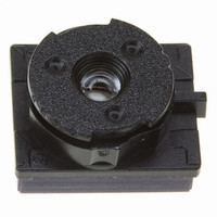
VS6502 9 Socket Mechanical Data 7,3 Socket Mechanical Data 10 1,5 10,5 45/48 ...
Page 46
Evaluation Hardware 10 Evaluation Hardware There is no ‘sensor only’ evaluation kit for the VS6502, however the daughtercard may be used with the evaluation kit for the SVTV676 and STVC674 coprocessors . Part Number VS6502V015 XS0015/TR STV-6502V-D01 STV-674/100T-E01 STV-676-E01 46/48 ...
Page 47
VS6502 Revision History Revision Date A April 2004 B 8th June 2004 Changes First version. Major changes. Second internal review and approval cycle via ADCS Evaluation Hardware 47/48 ...
Page 48
... No license is granted by implication or otherwise under any patent or patent rights of STMicroelectronics. Specifications mentioned in this publication are subject to change without notice. This publication supersedes and replaces all information previously supplied. STMicroelectronics products are not authorized for use as critical components in life support devices or systems without the The ST logo is a registered trademark of STMicroelectronics ...